
Datasheet


11
LTC1091/LTC1092
LTC1093/LTC1094
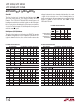
TEST CIRCUITS
Voltage Waveforms for t
en
1
LTC1092
CLK
D
OUT
t
en
B9
0.4V
1091/2/3/4 TC08
CS
CS
B9
D
OUT
t
en
0.4V
CLK
LTC1093/LTC1094
1091/2/3/4 TC09
START
7
4
563
2
1
D
IN
U
S
A
O
PP
L
IC
AT
I
WU
U
I FOR ATIO
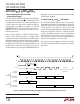
The LTC1091/LTC1092/LTC1093/LTC1094 are data
acquisiton components that contain the following func-
tional blocks:
1. 10-Bit Successive Approximation A/D Converter
2. Analog Multiplexer (MUX)
3. Sample-and-Hold (S/H)
4. Synchronous, Half-Duplex Serial Interface
5. Control and Timing Logic
DIGITAL CONSIDERATIONS
1. Serial Interface
The LTC1091/LTC1093/LTC1094 communicate with
microprocessors and other external circuitry via a syn-
chronous, half-duplex, 4-wire serial interface while the
LTC1092 uses a 3-wire interface (see Operating Sequence).
The clock (CLK) synchronizes the data transfer with each
bit being transmitted on the falling CLK edge and captured
on the rising CLK edge in both transmitting and receiving
systems. The LTC1091/LTC1093/LTC1094 first receive
input data and then transmit back the A/D conversion
result (half-duplex). Because of the half-duplex operation,
D
IN
and D
OUT
may be tied together allowing transmission
over just three wires: CS, CLK and DATA (D
IN
/D
OUT
).
Data transfer is initiated by a falling chip select (CS) signal.
After CS falls, the LTC1091/LTC1093/LTC1094 looks for a
start bit. After the start bit is received, a 3-bit input word
(6 bits for the LTC1093/LTC1094) is shifted into the D
IN
input which configures the LTC1091/LTC1093/LTC1094
and starts the conversion. After one null bit, the result of
the conversion is output on the D
OUT
line. At the end of the
data exchange, CS should be brought high. This resets the
LTC1091/LTC1093/LTC1094 in preparation for the next
data exchange.
The LTC1092 does not require a configuration input word
and has no D
IN
pin. A falling CS initiates data transfer as
shown in the LTC1092 Operating Sequence. After CS falls,