
Datasheet


9
LTC1091/LTC1092
LTC1093/LTC1094
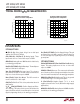
INPUT
SHIFT
REGISTER
SAMPLE-
AND-HOLD
10-BIT
CAPACITIVE
DAC
AV
CC
ANALOG
INPUT MUX
CH0
CH1
CH2
CH3
CH4
CH5
CH6
CH7
COM
D
OUT
CLK
CONTROL
AND
TIMING
CS
1091/2/3/4 BD
REF
+
DGND
AGND
V
–
REF
–
COMP
OUTPUT
SHIFT
REGISTER
D
IN
10-BIT
SAR
1
2
3
4
5
6
7
8
9
10
11 12 13 14
DV
CC
19
17
16
18
15
20
(Pin numbers refer to LTC1094)
BLOCK DIAGRA
W
V
REF
(Pin 11)(LTC1093): Reference Input. The reference
input must be kept free of noise with respect to AGND.
REF
+
, REF
–
(Pins 13, 14 )(LTC1094): Reference Input.
The reference input must be kept free of noise with respect
to AGND.
D
IN
(Pin 12/Pin 15): Data Input. The A/D configuration
word is shifted into this input.
D
OUT
(Pin 13/Pin 16): Digital Data Output. The A/D con-
version result is shifted out of this output.
CS (Pin 14/Pin 17): Chip Select Input. A logic low on this
input enables the LTC1093/LTC1094.
PI FU CTIO S
U
UU
CLK (Pin 15/Pin 18): Shift Clock. This clock synchronizes
the serial data transfer.
V
CC
(Pin 16)(LTC1093): Positive Supply. This supply
must be kept free of noise and ripple by bypassing directly
to the analog ground plane.
AV
CC
, DV
CC
(Pins 19, 20)(LTC1094): Positive Supply.
This supply must be kept free of noise and ripple by
bypassing directly to the analog ground plane. AV
CC
and
DV
CC
should be tied together on the LTC1094.