
Datasheet


24
LTC1091/LTC1092
LTC1093/LTC1094
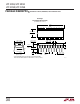
Figure 12. Reference Input Equivalent Circuit
U
S
A
O
PP
L
IC
AT
I
WU
U
I FOR ATIO
Differential Inputs
With differential inputs, the A/D no longer converts just a
single voltage but rather the difference between two volt-
ages. In this case, the voltage on the selected “+” input is still
sampled and held and therefore may be rapidly time varying
just as in single-ended mode. However, the voltage on the
selected “–” input must remain constant and be free of noise
and ripple throughout the conversion time. Otherwise, the
differencing operation may not be performed accurately.
The conversion time is 10 CLK cycles. Therefore, a change
in the “–” input voltage during this interval can cause
conversion errors. For a sinusoidal voltage on the “–” input
this error would be:
V
ERROR(MAX)
= (V
PEAK
)(2π) • f(“–”)(10/f
CLK
)
Where f(“–”) is the frequency of the “–” input voltage,
V
PEAK
is its peak amplitude and f
CLK
is the frequency of the
CLK. In most cases V
ERROR
will not be significant. For a
60Hz signal on the “–” input to generate a 0.25LSB error
(1.25mV) with the converter running at CLK = 500kHz, its
peak value would have to be 150mV.
5. Reference Inputs
The voltage between the reference inputs of the
LTC1091/LTC1092/LTC1093/LTC1094 defines the volt-
age span of the A/D converter. The reference inputs look
primarily like a 10k resistor but will have transient capaci-
tive switching currents due to the switched capacitor
conversion technique (see Figure 12). During each bit test
of the conversion (every CLK cycle), a capacitive current
spike will be generated on the reference pins by the A/D.
These current spikes settle quickly and do not cause a
problem. However, if slow settling circuitry is used to drive
the reference inputs, care must be taken to ensure that
transients caused by these current spikes settle com-
pletely during each bit test of the conversion.
When driving the reference inputs, three things should be
kept in mind:
1. The source resistance (R
OUT
) driving the reference
inputs should be low (less than 1Ω) to prevent DC
drops caused by the 1mA maximum reference current
(I
REF
).
2. Transients on the reference inputs caused by the
capacitive switching currents must settle completely
during each bit test (each CLK cycle). Figures 13 and
14 show examples of both adequate and poor settling.
Using a slower CLK will allow more time for the
reference to settle. However, even at the maximum
CLK rate of 500kHz most references and op amps can
be made to settle within the 2µs bit time.
3. It is recommended that the REF
–
input of the LTC1094
be tied directly to the analog ground plane. If REF
–
is
biased at a voltage other than ground, the voltage must
not change during a conversion cycle. This voltage
must also be free of noise and ripple with respect to
analog ground.
R
ON
5pF TO
30pF
10k
TYP
LTC1091/2/3/4
REF
+
R
OUT
V
REF
EVERY CLK CYCLE
14
13
(AGND)
1091-4 F12
0.5mV/DIV
1µs/DIV
1091-4 F13
Figure 13. Adequate Reference Settling