LTC1096/LTC1096L LTC1098/LTC1098L Micropower Sampling 8-Bit Serial I/O A/D Converters FEATURES DESCRIPTION n The LTC ® 1096/LTC1096L/LTC1098/LTC1098L are micropower, 8-bit A/D converters that draw only 80μA of supply current when converting. They automatically power down to 1nA typical supply current whenever they are not performing conversions. They are packaged in 8-pin SO packages and have both 3V (L) and 5V versions.
LTC1096/LTC1096L LTC1098/LTC1098L ABSOLUTE MAXIMUM RATINGS (Notes 1 and 2) Supply Voltage (VCC) to GND ...................................12V Voltage Analog and Reference ................ –0.3V to VCC + 0.3V Digital Inputs ........................................ –0.3V to 12V Digital Outputs ........................... –0.3V to VCC + 0.3V Power Dissipation ...............................................500mW Storage Temperature Range...................
LTC1096/LTC1096L LTC1098/LTC1098L ORDER INFORMATION LEAD BASED FINISH TAPE AND REEL PART MARKING* PACKAGE DESCRIPTION TEMPERATURE RANGE LTC1096ACN8 LTC1096ACN8#TR LTC1096ACN8 8-Lead Plastic DIP 0°C to 70°C LTC1096ACS8 LTC1096ACS8#TR 1096A 8-Lead Plastic SOIC 0°C to 70°C LTC1096AIN8 LTC1096AIN8#TR LTC1096AIN8 8-Lead Plastic DIP –40°C to 85°C LTC1096AIS8 LTC1096AIS8#TR 1096AI 8-Lead Plastic SOIC –40°C to 85°C LTC1096CN8 LTC1096CN8#TR LTC1096CN8 8-Lead Plastic DIP 0°C to 70°C LTC1
LTC1096/LTC1096L LTC1098/LTC1098L RECOMMENDED OPERATING CONDITIONS LTC1096/LTC1098 SYMBOL PARAMETER CONDITIONS tWHCS CS High Time Between Data Transfer Cycles VCC = 5V MIN 1 TYP MAX UNITS μs tWLCS CS Low Time During Data Transfer LTC1096, fCLK = 500kHz LTC1098, fCLK = 500kHz 28 28 μs μs VCC = 3V Operation fCLK Clock Frequency VCC = 3V 25 tCYC Total Cycle Time LTC1096, fCLK = 250kHz LTC1098, fCLK = 250kHz 58 58 250 kHz μs μs thDI Hold Time, DIN After CLK↑ VCC = 3V 450 ns tsuCS
LTC1096/LTC1096L LTC1098/LTC1098L CONVERTER AND MULTIPLEXER CHARACTERISTICS LTC1096/LTC1098 The l denotes the specifications which apply over the full operating temperature range, otherwise specifications are at TA = 25°C. VCC = 5V, VREF = 5V, fCLK = 500kHz, unless otherwise noted. LTC1096A/LTC1098A PARAMETER CONDITIONS MIN TYP LTC1096/LTC1098 MAX MIN TYP MAX UNITS Resolution (No Missing Code) l Offset Error l ±0.5 ±0.5 LSB l ±0.5 ±0.5 LSB l ±0.5 ±1.0 LSB l ±0.5 ±1.
LTC1096/LTC1096L LTC1098/LTC1098L DIGITAL AND DC ELECTRICAL CHARACTERISTICS LTC1096/LTC1098 The l denotes the specifications which apply over the full operating temperature range, otherwise specifications are at TA = 25°C. VCC = 5V, VREF = 5V, unless otherwise noted. SYMBOL PARAMETER CONDITIONS MIN VIH High Level Input Voltage VCC = 5.25V l VIL Low Level Input Voltage VCC = 4.
LTC1096/LTC1096L LTC1098/LTC1098L DIGITAL AND DC ELECTRICAL CHARACTERISTICS LTC1096L/LTC1098L The l denotes the specifications which apply over the full operating temperature range, otherwise specifications are at TA = 25°C. VCC = 2.65V, VREF = 2.5V, fCLK = 250kHz, unless otherwise noted. SYMBOL PARAMETER CONDITIONS MIN VIH High Level Input Voltage VCC = 3.6V l VIL Low Level Input Voltage VCC = 2.65V l TYP MAX UNITS 0.45 V 1.9 V IIH High Level Input Current VIN = VCC l 2.
LTC1096/LTC1096L LTC1098/LTC1098L AC CHARACTERISTICS LTC1096/LTC1098 The l denotes the specifications which apply over the full operating temperature range, otherwise specifications are at TA = 25°C. VCC = 3V, VREF = 2.5V, fCLK = 250kHz, unless otherwise noted. SYMBOL PARAMETER CONDITIONS MIN tSMPL Analog Input Sample Time See Operating Sequence MAX 1.5 l fSMPL(MAX) Maximum Sampling Frequency TYP UNITS CLK Cycles 16.
LTC1096/LTC1096L LTC1098/LTC1098L TYPICAL PERFORMANCE CHARACTERISTICS Supply Current vs Clock Rate for Active and Shutdown Modes VCC = 9V SUPPLY CURRENT, ICC (μA) 150 VCC = 5V 100 50 10 0.002 0 CS = VCC 80 60 “ACTIVE” MODE CS = 0 40 20 0 1 7 3 2 5 6 4 SUPPLY VOLTAGE,VCC (V) Change in Offset vs Reference Voltage LTC1096 0.25 0 1 0 0.50 0.3 0.2 0.1 0 –0.1 –0.2 –0.3 0 1 2 3 4 5 6 7 8 SUPPLY VOLTAGE, VCC (V) 10968 G04 Change in Linearity vs Supply Voltage 0.25 0 –0.25 9 10 –O.
LTC1096/LTC1096L LTC1098/LTC1098L TYPICAL PERFORMANCE CHARACTERISTICS Maximum Clock Frequency vs Source Resistance Maximum Clock Frequency vs Supply Voltage 1.5 VIN + INPUT – INPUT 0.75 RSOURCE– 0.50 0.25 0 1.25 10 RSOURCE– (kΩ) 0.75 0.5 0 2 Minimum Wake-Up Time vs Source Resistance 1 7.5 5.0 RSOURCE+ VIN 2.5 100 + 10 ON CHANNEL 1 10 1 0.01 –60 –40 –20 0 20 40 60 80 100 120 140 TEMPERATURE (°C) 100 RSOURCE (kΩ) 10968 G14 10968 G13 Minimum Clock Frequency for 0.
LTC1096/LTC1096L LTC1098/LTC1098L PIN FUNCTIONS LTC1096/LTC1096L LTC1098/LTC1098L CS/SHDN (Pin 1): Chip Select Input. A logic low on this input enables the LTC1096/LTC1096L. A logic high on this input disables the LTC1096/LTC1096L and disconnects the power to the LTC1096/LTC1096L. CS/SHDN (Pin 1): Chip Select Input. A logic low on this input enables the LTC1098/LTC1098L. A logic high on this input disables the LTC1098/LTC1098L and disconnects the power to the LTC1098/LTC1098L. IN+ (Pin 2): Analog Input.
LTC1096/LTC1096L LTC1098/LTC1098L BLOCK DIAGRAM LTC1096/LTC1096L CS (DIN) CLK VCC (VCC/VREF) BIAS AND SHUTDOWN CIRCUIT IN+ (CH0) CSAMPLE IN– (CH1) SERIAL PORT DOUT – SAR + MICROPOWER COMPARATOR CAPACITIVE DAC 10968 BD GND VREF PIN NAMES IN PARENTHESES REFER TO THE LTC1098/LTC1098L TEST CIRCUITS On and Off Channel Leakage Current Load Circuit for tdDO, tr and tf 5V ION 1.
LTC1096/LTC1096L LTC1098/LTC1098L TEST CIRCUITS Voltage Waveforms for DOUT Delay Time, tdDO CLK Voltage Waveforms for DOUT Rise and Fall Times, tr, tf VIL VOH DOUT tdDO VOL VOH DOUT tr VOL tf 10968 TC04 10968 TC03 Load Circuit for tdis and ten Voltage Waveforms for tdis CS 2.
LTC1096/LTC1096L LTC1098/LTC1098L TEST CIRCUITS Voltage Waveforms for ten LTC1096/LTC1096L CS tWAKEUP 1 CLK B7 DOUT VOL ten 10968 TC07 LTC1098/LTC1098L CS START DIN CLK 1 2 3 4 5 B7 DOUT VOL ten 10968 TC08 10968fc 14
LTC1096/LTC1096L LTC1098/LTC1098L APPLICATIONS INFORMATION OVERVIEW The LTC1096/LTC1096L/LTC1098/LTC1098L are 8-bit micropower, switched-capacitor A/D converters. These sampling ADCs typically draw 120μA of supply current when sampling up to 33kHz. Supply current drops linearly as the sample rate is reduced (see Supply Current vs Sample Rate on the first page of this data sheet). The ADCs automatically power down when not performing conversion, drawing only leakage current.
LTC1096/LTC1096L LTC1098/LTC1098L APPLICATIONS INFORMATION tCYC CS POWER DOWN CLK tsuCS tWAKEUP DOUT HI-Z NULL BIT B7 B6 (MSB) B5 B4 B3 B2 Hi-Z B0 B1 tCONV tCYC CS POWER DOWN CLK tsuCS tWAKEUP DOUT Hi-Z NULL BIT B7 (MSB) B6 B5 B4 B3 B2 B0 B1 B1 B2 B3 B4 B5 B6 B7* tCONV Hi-Z 10968 F01 *AFTER COMPLETING THE DATA TRANSFER, IF FURTHER CLOCKS ARE APPLIED WITH CS LOW, THE ADC WILL OUTPUT ZEROS INDEFINITELY. Figure 1.
LTC1096/LTC1096L LTC1098/LTC1098L APPLICATIONS INFORMATION MSB-FIRST DATA (MSBF = 1) tCYC CS POWER DOWN tWAKEUP CLK tsuCS ODD/ SIGN START DIN DON'T CARE MSBF SGL/ DIFF DOUT NULL BIT B7 B6 (MSB) HI-Z tSMPL B5 B4 B3 B2 B1 Hi-Z B0* tCONV MSB-FIRST DATA (MSBF = 0) tCYC CS POWER DOWN tWAKEUP CLK tsuCS ODD/ SIGN START DIN DON'T CARE SGL/ DIFF DOUT HI-Z tSMPL MSBF NULL B6 BIT B7 (MSB) B5 B4 B3 B2 B1 B0 B1 B2 B3 B4 B5 B6 B7* tCONV Hi-Z 10968 F02 *AFTER COMPLETING THE DATA T
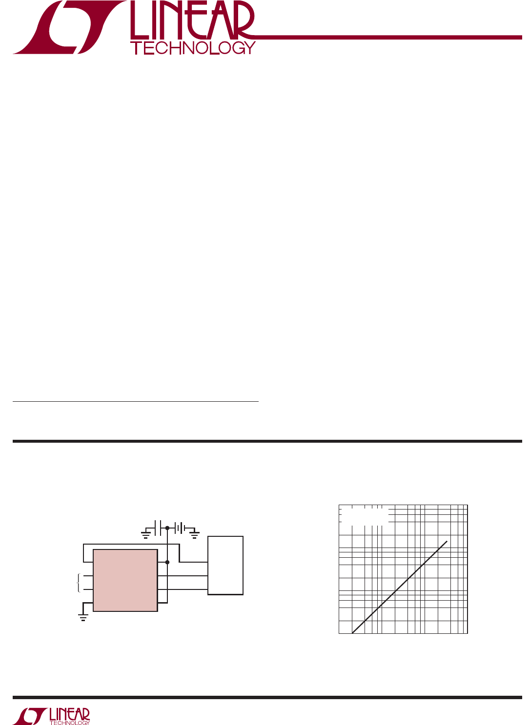
LTC1096/LTC1096L LTC1098/LTC1098L APPLICATIONS INFORMATION Multiplexer (MUX) Address Unipolar Transfer Curve The bits of the input word following the START bit assign the MUX configuration for the requested conversion. For a given channel selection, the converter will measure the voltage between the two channels indicated by the “+” and “–” signs in the selected row of the followintg tables. In single-ended mode, all input channels are measured with respect to GND.
LTC1096/LTC1096L LTC1098/LTC1098L APPLICATIONS INFORMATION MSBF BIT LATCHED BY LTC1098(L) CS 1 2 3 4 START SGL/DIFF ODD/SIGN MSBF CLK DATA (DIN/DOUT) B7 MPU CONTROLS DATA LINE AND SENDS MUX ADDRESS TO LTC1098(L) • • • B6 LTC1098(L) CONTROLS DATA LINE AND SENDS A/D RESULT BACK TO MPU PROCESSOR MUST RELEASE DATA LINE AFTER 4TH RISING CLK AND BEFORE THE 4TH FALLING CLK LTC1098(L) TAKES CONTROL OF DATA LINE ON 4TH FALLING CLK 10968 F03 Figure 3.
LTC1096/LTC1096L LTC1098/LTC1098L APPLICATIONS INFORMATION of the converter will draw current. This current may be larger than the typical supply current. It is worthwhile to bring the CS pin all the way to ground when it is low and all the way to supply voltage when it is high to obtain the lowest supply current. When the CS pin is high (= supply voltage), the converter is in shutdown mode and draws only leakage current. The status of the DIN and CLK input have no effect on supply current during this time.
LTC1096/LTC1096L LTC1098/LTC1098L APPLICATIONS INFORMATION (Figure 6) and connect the center point to the MPU input. It should be noted that to get full shutdown, the CS input of the LTC1096/LTC1098 must be driven to the VCC voltage. This would require adding a level shift circuit to the CS signal in Figure 6. 9V OPTIONAL LEVEL SHIFT 9V 4.7μF SAMPLE-AND-HOLD MPU (e.g. 8051) DIFFERENTIAL INPUTS COMMON MODE RANGE 0V TO 6V CS VCC +IN CLK –IN DOUT GND VREF 5V P1.4 P1.3 50k P1.
LTC1096/LTC1096L LTC1098/LTC1098L APPLICATIONS INFORMATION in and continues until the falling CLK edge after the MSBF bit is received. On this falling edge, the S&H goes into hold mode and the conversion begins. Differential Inputs With differential inputs, the ADC no longer converts just a single voltage but rather the difference between two voltages. In this case, the voltage on the selected “+” input is still sampled and held and therefore may be rapidly time varying just as in single-ended mode.
LTC1096/LTC1096L LTC1098/LTC1098L APPLICATIONS INFORMATION Large external source resistors and capacitances will slow the settling of the inputs. It is important that the overall RC time constants be short enough to allow the analog inputs to completely settle within the allowed time. RC Input Filtering It is possible to filter the inputs with an RC network as shown in Figure 9. For large values of CF (e.g., 1μF), the capacitive input switching currents are averaged into a net DC current.
LTC1096/LTC1096L LTC1098/LTC1098L APPLICATIONS INFORMATION Noise with Reduced VREF The total input referred noise of the LTC1096 can be reduced to approximately 1mV peak-to-peak using a ground plane, good bypassing, good layout techniques and minimizing noise on the reference inputs. This noise is insignificant with a 5V reference but will become a larger fraction of an LSB as the size of the LSB is reduced. For operation with a 5V reference, the 1mV noise is only 0.05LSB peak-to-peak.
LTC1096/LTC1096L LTC1098/LTC1098L APPLICATIONS INFORMATION Effective Number of Bits EFFECTIVE NUMBER OF BITS (ENOBs) 8 The effective number of bits (ENOBs) is a measurement of the resolution of an A/D and is directly related to the S/(N + D) by the equation: ENOB = [S/(N + D) –1.76]/6.02 where S/(N + D) is expressed in dB. At the maximum sampling rate of 33kHz the LTC1096 maintains 7.5 ENOBs or better to 40kHz.
LTC1096/LTC1096L LTC1098/LTC1098L TYPICAL APPLICATIONS Data Exchange Between LTC1098(L) and MC68HC05C4 START BIT MPU TRANSMIT WORD 0 0 0 BYTE 1 SGL/ ODD/ MSBF X DIFF SIGN 1 BYTE 2 (DUMMY) X X X X X X X X X = DON'T CARE CS START SGL/ ODD/ DIFF SIGN MSBF DIN DON'T CARE CLK DOUT MPU RECEIVED WORD ? ? ? ? ? ? ? 0 B7 B6 B5 B4 B3 B2 B1 B0 B7 B6 B5 B4 B3 B2 B1 B0 1ST TRANSFER Hardware and Software Interface to Motorola MC68HC05C4 CS C0 SCK MC68HC05C4 MISO CLK ANALO
LTC1096/LTC1096L LTC1098/LTC1098L TYPICAL APPLICATIONS Interfacing to the Parallel Port of the Intel 8051 Family LABEL The Intel 8051 has been chosen to demonstrate the interface between the LTC1098(L) and parallel port microprocessors. Normally the CS, CLK and DIN signals would be generated on three port lines and the DOUT signal read on a fourth port line. This works very well.
LTC1096/LTC1096L LTC1098/LTC1098L A “Quick Look” Circuit for the LTC1096 Users can get a quick look at the function and timing of the LT1096 by using the following simple circuit (Figure 13). VREF is tied to VCC. VIN is applied to the +IN input and the – IN input is tied to the ground. CS is driven at 1/16 the clock rate by the 74C161 and DOUT outputs the data. The output data from the DOUT pin can be viewed on an oscilloscope that is set up to trigger on the falling edge of CS (Figure 14).
LTC1096/LTC1096L LTC1098/LTC1098L Remote or Isolated Systems Figure 16 shows a floating system that sends data to a grounded host system. The floating circuitry is isolated by two optoisolators and powered by a simple capacitor diode charge pump. The system has very low power requirements because the LTC1096 shuts down between conversions and the optoisolators draw power only when data is being transferred. The system consumes only 50μA at a sample rate of 10Hz (1ms on-time and 99ms off-time).
LTC1096/LTC1096L LTC1098/LTC1098L PACKAGE DESCRIPTION N8 Package 8-Lead PDIP (Narrow .300 Inch) (Reference LTC DWG # 05-08-1510) .400* (10.160) MAX 8 7 6 5 1 2 3 4 .255 ± .015* (6.477 ± 0.381) .300 – .325 (7.620 – 8.255) .008 – .015 (0.203 – 0.381) ( +.035 .325 –.015 8.255 +0.889 –0.381 ) .045 – .065 (1.143 – 1.651) .130 ± .005 (3.302 ± 0.127) .065 (1.651) TYP .100 (2.54) BSC .120 (3.048) .020 MIN (0.508) MIN .018 ± .003 (0.457 ± 0.076) N8 1002 NOTE: 1.
LTC1096/LTC1096L LTC1098/LTC1098L PACKAGE DESCRIPTION S8 Package 8-Lead Plastic Small Outline (Narrow .150 Inch) (Reference LTC DWG # 05-08-1610) .189 – .197 (4.801 – 5.004) NOTE 3 .045 ±.005 .050 BSC 8 .245 MIN 7 6 5 .160 ±.005 .150 – .157 (3.810 – 3.988) NOTE 3 .228 – .244 (5.791 – 6.197) .030 ±.005 TYP 1 RECOMMENDED SOLDER PAD LAYOUT .010 – .020 × 45° (0.254 – 0.508) .008 – .010 (0.203 – 0.254) 3 4 .053 – .069 (1.346 – 1.752) .004 – .010 (0.101 – 0.254) 0°– 8° TYP .016 – .050 (0.406 – 1.
LTC1096/LTC1096L LTC1098/LTC1098L TYPICAL APPLICATION A/D Conversion for 3V Systems The LTC1096/LTC1098 are ideal for 3V systems. Figure 17 shows a 3V to 6V battery current monitor that draws only 70μA from the battery it monitors. The battery current is sensed with the 0.02Ω resistor and amplified by the LT1178. The LTC1096 digitizes the amplifier output and sends it to the microprocessor in serial format. The LT1004 provides the full-scale reference for the ADC.