
Datasheet


LTC1096/LTC1096L
LTC1098/LTC1098L
8
10968fc
Note 1: Stresses beyond those listed under Absolute Maximum Ratings
may cause permanent damage to the device. Exposure to any Absolute
Maximum Rating condition for extended periods may affect device
reliability and lifetime.
Note 2: All voltage values are with respect to GND.
Note 3: For the 8-lead PDIP, consult the factory.
Note 4: Linearity error is specifi ed between the actual and points of the
A/D transfer curve.
Note 5: Total unadjusted error includes offset, full scale, linearity,
multiplexer and hold step errors.
Note 6: Two on-chip diodes are tied to each reference and analog input
which will conduct for reference or analog input voltages one diode
drop below GND or one diode drop above V
CC
. This spec allows 50mV
forward bias of either diode. This means that as long as the reference or
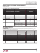
SYMBOL PARAMETER CONDITIONS MIN TYP MAX UNITS
t
SMPL
Analog Input Sample Time See Operating Sequence 1.5 CLK Cycles
f
SMPL(MAX)
Maximum Sampling Frequency
l
16.5 kHz
t
CONV
Conversion Time See Operating Sequence 8 CLK Cycles
t
dDO
Delay Time, CLK↓ to D
OUT
Data Valid
See Test Circuits (Note 9)
l
500 1000 ns
t
dis
Delay Time, CS↑ to D
OUT
Hi-Z
See Test Circuits (Note 9)
l
220 800 ns
t
en
Delay Time, CLK↓ to D
OUT
Enable
See Test Circuits (Note 9)
l
160 480 ns
t
hDO
Time Output Data Remains Valid After CLK↓
C
LOAD
= 100pF 400 ns
t
f
D
OUT
Fall Time See Test Circuits (Note 9)
l
70 250 ns
t
r
D
OUT
Rise Time See Test Circuits (Note 9)
l
50 150 ns
C
IN
Input Capacitance Analog Inputs On Channel
Analog Inputs Off Channel
25
5
pF
pF
Digital Input 5 pF
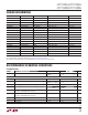
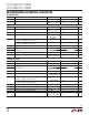
AC CHARACTERISTICS
LTC1096/LTC1098
The l denotes the specifi cations which apply over the full operating temperature range, otherwise specifi cations are at T
A
= 25°C.
V
CC
= 3V, V
REF
= 2.5V, f
CLK
= 250kHz, unless otherwise noted.
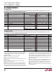
SYMBOL PARAMETER CONDITIONS MIN TYP MAX UNITS
t
SMPL
Analog Input Sample Time See Operating Sequence 1.5 CLK Cycles
f
SMPL(MAX)
Maximum Sampling Frequency
l
16.5 kHz
t
CONV
Conversion Time See Operating Sequence 8 CLK Cycles
t
dDO
Delay Time, CLK↓ to D
OUT
Data Valid
See Test Circuits
l
500 1000 ns
t
dis
Delay Time, CS↑ to D
OUT
Hi-Z
See Test Circuits
l
220 800 ns
t
en
Delay Time, CLK↓ to D
OUT
Enable
See Test Circuits
l
160 480 ns
t
hDO
Time Output Data Remains Valid After CLK↓
C
LOAD
= 100pF 400 ns
t
f
D
OUT
Fall Time See Test Circuits
l
70 250 ns
t
r
D
OUT
Rise Time See Test Circuits
l
50 200 ns
C
IN
Input Capacitance Analog Inputs On Channel
Analog Inputs Off Channel
25
5
pF
pF
Digital Input 5 pF
LTC1096L/LTC1098L
The l denotes the specifi cations which apply over the full operating temperature range, otherwise specifi cations are at T
A
= 25°C.
V
CC
= 2.65V, V
REF
= 2.5V, f
CLK
= 250kHz, unless otherwise noted.
analog input does not exceed the supply voltage by more than 50mV, the
output code will be correct. To achieve an absolute 0V to 5V input voltage
range will therefore require a minimum supply voltage of 4.950V over
initial tolerance, temperature variations and loading. For 5.5V < V
CC
≤ 9V,
reference and analog input range cannot exceed 5.55V. If reference and
analog input range are greater than 5.55V, the output code will not be
guaranteed to be correct.
Note 7: The supply voltage range for the LTC1096L/LTC1098L is from
2.65V to 4V. The supply voltage range for the LTC1096 is from 3V to 9V,
but the supply voltage range for the LTC1098 is only from 3V to 6V.
Note 8: Channel leakage current is measured after the channel selection.
Note 9: These specifi cations are either correlated from 5V specifi cations or
guaranteed by design.