
Datasheet


11
LTC1147-3.3
LTC1147-5/LTC1147L
sn1147 1147fds
where L1, L2, etc., are the individual losses as a percent-
age of input power. (For high efficiency circuits only small
errors are incurred by expressing losses as a percentage
of output power.)
Although all dissipative elements in the circuit produce
losses, four main sources usually account for most of the
losses in LTC1147 circuits: 1) LTC1147 DC bias current,
2) MOSFET gate charge current, 3) I
2
R losses, and 4)
voltage drop of the Schottky diode.
1. The DC supply current is the current which flows into
V
IN
(Pin 1) less the gate charge current. For V
IN
= 10V
the LTC1147 series DC supply current is 160µA for no
load, and increases proportionally with load up to a
constant 1.6mA after the LTC1147 series has entered
continuous mode. Because the DC bias current is
drawn from V
IN
, the resulting loss increases with
input voltage. For V
IN
= 10V the DC bias losses are
generally less than 1% for load currents over 30mA.
However, at very low load currents the DC bias current
accounts for nearly all of the loss.
2. MOSFET gate charge current results from switching
the gate capacitance of the power MOSFET. Each time
a MOSFET gate is switched from low to high to low
again, a packet of charge dQ moves from V
IN
to
ground. The resulting dQ/dt is a current out of V
IN
which is typically much larger than the DC supply
current. In continuous mode, I
GATECHG
= f(Q
P
). The
typical gate charge for a 0.135Ω P-channel power
MOSFET is 40nC. This results in I
GATECHG
= 4mA in
100kHz continuous operation for a 2% to 3% typical
midcurrent loss with V
IN
= 10V.
Note that the gate charge loss increases directly with
both input voltage and operating frequency. This is the
principal reason why the highest efficiency circuits
operate at moderate frequencies. Furthermore, it ar-
gues against using a larger MOSFET than necessary to
control I
2
R losses, since overkill can cost efficiency as
well as money!
3. I
2
R losses are easily predicted from the DC resis-
tances of the MOSFET, inductor and current shunt. In
continuous mode the average output current flows
through L and R
SENSE
, but is “chopped” between the
P-channel and Schottky diode. The MOSFET R
DS(ON)
multiplied by the P-channel duty cycle can be summed
with the resistances of L and R
SENSE
to obtain I
2
R
losses. For example, if R
DS(ON)
= 0.1Ω, R
L
= 0.15Ω,
and R
SENSE
= 0.05Ω, then the total
resistance is 0.3Ω
at V
IN
≈ 2V
OUT
. This results in losses ranging from 3%
to 10% as the output current increases from 0.5A to
2A. I
2
R losses cause the efficiency to roll off at high
output currents.
4. The Schottky diode is a major source of power loss at
high currents and gets worse at high input voltages.
The diode loss is calculated by multiplying the forward
voltage drop times the Schottky diode duty cycle
multiplied by the load current. For example, assuming
a duty cycle of 50% with a Schottky diode forward
voltage drop of 0.4V, the loss increases from 0.5% to
8% as the load current increases from 0.5A to 2A.
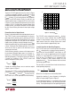
Figure 5 shows how the efficiency losses in a typical
LTC1147 series regulator end up being apportioned.
The gate charge loss is responsible for the majority of
the efficiency lost in the midcurrent region. If Burst
Mode
operation was not employed at low currents,
the gate charge loss alone would cause efficiency to
drop to unacceptable levels. With Burst Mode
opera-
tion, the DC supply current represents the lone (and
unavoidable) loss component which continues to
become a higher percentage as output current is
reduced. As expected, the I
2
R losses and Schottky
diode loss dominate at high load currents.
Figure 5. Efficiency Loss
OUTPUT CURRENT (A)
0.01
EFFICIENCY/LOSS (%)
90
95
1
LTC1147 • F05
85
80
0.03
0.1
0.3
3
100
GATE CHARGE
LTC1147 I
Q
I
2
R
SCHOTTKY
DIODE
APPLICATIO S I FOR ATIO
WUU
U