
Datasheet


5
LTC1147-3.3
LTC1147-5/LTC1147L
sn1147 1147fds
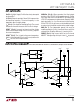
V
IN
(Pin 1): Main Supply Pin. Must be closely decoupled
to ground Pin 7.
C
T
(Pin 2): External capacitor C
T
from Pin 2 to ground sets
the operating frequency. The actual frequency is also
dependent upon the input voltage.
I
TH
(Pin 3): Gain Amplifier Decoupling Point. The current
comparator threshold increases with the Pin 3 voltage.
SENSE
–
(Pin 4): Connects to internal resistive divider
which sets the output voltage. Pin 4 is also the (–) input for
the current comparator.
SENSE
+
(Pin 5): The (+) input to the current comparator.
A built-in offset between Pins 4 and 5 in conjunction with
R
SENSE
sets the current trip threshold.
SHDN/V
FB
(Pin 6): When grounded, the fixed output
versions of the LTC1147 family operate normally. Pulling
Pin 6 high holds the P-channel MOSFET off and puts the
LTC1147 in micropower shutdown mode. Requires CMOS
logic signal with t
r
, t
f
< 1µs. Do not leave this pin floating.
On the LTC1147L this pin serves as the feedback pin from
an external resistive divider used to set the output voltage.
GND (Pin 7): Two independent ground lines must be
routed separately to: 1) the (–) terminal of C
OUT
, and 2) the
cathode of the Schottky diode and (–) terminal of C
IN
.
PDRIVE (Pin 8): High current drive for the P-channel
MOSFET. Voltage swing at this pin is from V
IN
to ground.
Pin 6 Connection Shown For LTC1147-3.3 and LTC1147-5; Changes Create LTC1147L.
+
–
1
PDRIVE
V
IN
GND
R
S
Q
–
+
C
25mV TO 150mV
3
13k
I
TH
1.25V
6
REFERENCE
–
+
SHDN
V
OS
–
+
V
G
5
6
SENSE
+
100k
5pF
–
+
V
TH1
T
–
+
V
TH2
S
SLEEP
2
C
T
OFF-TIME
CONTROL
V
IN
SENSE
–
SENSE
–
4
8
7
LTC1147 • FD
V
FB
PI FU CTIO S
UUU
FU CTIO AL DIAGRA
UUW