
Datasheet


9
LTC1147-3.3
LTC1147-5/LTC1147L
sn1147 1147fds
used. For V
IN
> 8V, a standard threshold MOSFET (V
GS(TH)
< 4V) may be used. If V
IN
is expected to drop below 8V,
a logic-level threshold MOSFET (V
GS(TH)
< 2.5V) is
strongly recommended. When a logic-level MOSFET is
used, the LTC1147 supply voltage must be less than the
absolute maximum V
GS
ratings for the MOSFET.
The maximum output current I
MAX
determines the R
DS(ON)
requirement for the power MOSFET. When the LTC1147
series is operating in continuous mode, the simplifying
assumption can be made that either the MOSFET or
Schottky diode is always conducting the average load
current. The duty cycles for the MOSFET and diode are
given by:
P-Ch Duty Cycle =
V
OUT
V
IN
Schottky Diode Duty Cycle =
(V
IN
– V
OUT
+ V
D
)
V
IN
From the duty cycle the required R
DS(ON)
for the MOSFET
can be derived:
P-Ch R
DS(ON)
=
(V
IN
)(P
P
)
(V
OUT
)(I
MAX
2
)(1 + δ
P
)
where P
P
is the allowable power dissipation and δ
P
is the
temperature dependency of R
DS(ON)
. P
P
will be deter-
mined by efficiency and/or thermal requirements (see
Efficiency Considerations). (1 + δ) is generally given for a
MOSFET in the form of a normalized R
DS(ON)
vs tempera-
ture curve, but δ = 0.007/°C can be used as an approxima-
tion for low voltage MOSFETs.
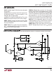
Output Diode Selection (D1)
The Schottky diode D1 shown in Figure 1 only conducts
during the off-time. It is important to adequately specify
the diode peak current and average power dissipation so
as not to exceed the diode ratings.
The most stressful condition for the output diode is under
short circuit (V
OUT
= 0V). Under this condition the diode
must safely handle I
SC(PK)
at close to 100% duty cycle.
Under normal load conditions the average current con-
ducted by the diode is:
(V
IN
– V
OUT
+ V
D
)
V
IN
(I
LOAD
)I
D1
=
Remember to keep lead lengths short and observe proper
grounding (see Board Layout Checklist) to avoid ringing
and increased dissipation.
The forward voltage drop allowable in the diode is calcu-
lated from the maximum short-circuit current as:
V
F
≈
P
D
I
SC(PK)
where P
D
is the allowable power dissipation and will be
determined by efficiency and/or thermal requirements
(see Efficiency Considerations).
C
IN
and C
OUT
Selection
In continuous mode, the source current of the P-channel
MOSFET is a square wave of duty cycle V
OUT
/V
IN
. To
prevent large voltage transients, a low ESR input capaci-
tor sized for the
maximum RMS current must be used. The
maximum RMS capacitor current is given by:
C
IN
Required I
RMS
≈ I
MAX
[V
OUT
(V
IN
–
V
OUT
)]
1/2
V
IN
This formula has a maximum at V
IN
= 2V
OUT
, where
I
RMS
= I
OUT
/2. This simple worst-case condition is com-
monly used for design because even significant devia-
tions do not offer much relief. Note that capacitor
manufacturer’s ripple current ratings are often based on
only 2000 hours of life. This makes it advisable to further
derate the capacitor, or to choose a capacitor rated at a
higher temperature than required. Several capacitors
may also be paralleled to meet size or height require-
ments in the design. Always consult the manufacturer if
there is any question. An additional 0.1µF to 1µF ceramic
decoupling capacitor is also required on V
IN
(Pin 1) for
high frequency decoupling.
The selection of C
OUT
is driven by the required effective
series resistance (ESR).
The ESR of C
OUT
must be less
than twice the value of R
SENSE
for proper operation of the
LTC1147:
C
OUT
Required ESR < 2R
SENSE
APPLICATIO S I FOR ATIO
WUU
U