
Datasheet


8
LTC1149
LTC1149-3.3/LTC1149-5
APPLICATIO S I FOR ATIO
WUU U
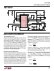
Figure 3. Timing Capacitor Selection
L and C
T
Selection for Operating Frequency
The LTC1149 series uses a constant off-time architecture
with t
OFF
determined by an external timing capacitor C
T
.
Each time the P-channel MOSFET switch turns on, the
voltage on C
T
is reset to approximately 3.3V. During the
off-time, C
T
is discharged by a current which is propor-
tional to V
OUT
. The voltage on C
T
is analogous to the
current in inductor L, which likewise decays at a rate
proportional to V
OUT
. Thus the inductor value must track
the timing capacitor value.
The value of C
T
is calculated from the desired continuous
mode operating frequency, f:
C
T
=
(7.8)(10
–5
)
f
)
)
1 –
V
OUT
V
IN
A graph for selecting C
T
versus frequency including the
effects of input voltage is given in Figure 3.
As the operating frequency is increased the gate charge
losses will be higher, reducing efficiency (see Efficiency
Considerations). The complete expression for operating
frequency is given by:
f =
1
t
OFF
)
)
1 –
V
OUT
V
IN
where:
t
OFF
= (1.3)(10
4
)(C
T
)
)
)
V
REG
V
OUT
V
REG
is the desired output voltage (i.e., 5V, 3.3V), while
V
OUT
is the actual output voltage. Thus V
REG
/V
OUT
= 1
when in regulation.
Note that as V
IN
decreases, the frequency decreases.
When the input to output voltage differential drops below
1.5V, the LTC1149 series reduces t
OFF
by increasing the
discharge current in C
T
. This prevents audible operation
prior to dropout.
Once the frequency has been set by C
T
, the inductor L must
be chosen to provide no more than 25mV/R
SENSE
of peak-
to-peak inductor ripple current. This results in a minimum
required inductor value of:
L
MIN
=( 5.1)(10
5
)(R
SENSE
)(C
T
)(V
REG
)
As the inductor value is increased from the minimum
value, the ESR requirements for the output capacitor are
eased at the expense of efficiency. If too small an inductor
is used, the inductor current will decrease past zero and
change polarity. A consequence of this is that the LTC1149
series may not enter Burst Mode
operation and efficiency
will be severely degraded at low currents.
FREQUENCY (kHz)
0
0
C
T
CAPACITANCE (pF)
200
400
600
1400
1000
50
100
1200
800
150
200
250
V
OUT
= 5V
V
IN
= 48V
V
IN
= 12V
V
IN
= 24V
1149 F03
The LTC1149 series automatically extends t
OFF
during a
short circuit to allow sufficient time for the inductor
current to decay between switch cycles. The resulting
ripple current causes the average short-circuit current
I
SC(AVG)
to be reduced to approximately I
MAX
.
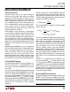
Figure 2. R
SENSE
vs Maximum Output Current
MAXIMUM OUTPUT CURRENT (A)
0
R
SENSE
(Ω)
0.12
0.16
0.20
4
1149 F02
0.08
0.04
0
1
2
3
5
0.10
0.14
0.18
0.06
0.02