
Datasheet


11
LTC1174
LTC1174-3.3/LTC1174-5
1174fe
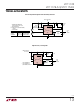
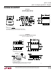
Figure 7. LTC1174 Layout Diagram (See Board Layout Checklist)
APPLICATIO S I FOR ATIO
WUUU
Board Layout Checklist
When laying out the printed circuit board, the following
checklist should be used to ensure proper operation of the
LTC1174. These items are also illustrated graphically in
the layout diagram in Figure 7. Check the following in your
layout:
1. Is the Schottky catch diode
closely
connected between
ground (Pin 4) and switch (Pin 5)?
2. Is the “+” plate of C
IN
closely
connected to V
IN
(Pin 6)?
This capacitor provides the AC current to the internal
P-channel MOSFET.
3. Is the 0.1µF V
IN
decoupling capacitor
closely
conected
between V
IN
(Pin 6) and ground (Pin 4)? This capacitor
carries the high frequency peak currents.
4. Is the SHUTDOWN (Pin 8) actively pulled to V
IN
during
normal operation? The SHUTDOWN pin is high imped-
ance and must not be allowed to float.
5. Is the I
PGM
(Pin 7) pulled either to V
IN
or ground? The
I
PGM
pin is high impedance and must not be allowed
to float.
3
LTC1174
2
SW
R1
8
7
6
1
54
L
V
OUT
D
1174 F07
OUTPUT DIVIDER
REQUIRED WITH
ADJUSTABLE
VERSION ONLY
0.1µF
LB
OUT
LB
IN
GND
SHUTDOWN
I
PGM
V
IN
R2
BOLD LINES INDICATE
HIGH CURRENT PATH
V
IN
C
IN
C
OUT
V
OUT
(V
FB
)
+
+
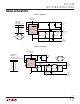
DESIGN EXAMPLE
As a design example, assume V
IN
= 9V (nominal), V
OUT
=
5V, and I
OUT
= 350mA maximum. The LTC1174-5 is used
for this application, with I
PGM
(Pin 7) connected to V
IN
. The
minmum value of L is determined by assuming the
LTC1174-5 is operating in continuous mode.
Figure 8. Continuous Inductor Current
INDUCTOR CURRENT
TIME
I
PEAK
I
V
AVG CURRENT
= I
OUT
=
= 350mA
I
PEAK
+ I
V
2
1174 F08
With I
OUT
= 350mA and I
PEAK
= 0.6A (I
PGM
= V
IN
), I
V
=
0.1A.The peak-to-peak ripple inductor current, I
RIPPLE
, is
0.5A and is also equal to:
I
VV
L
A
RIPPLE
OUT D
PP
=
+
⎛
⎝
⎜
⎞
⎠
⎟
()
−
−
410
6
•