
Datasheet


LTC1196/LTC1198
6
119698fb
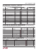
DIGITAL AND DC ELECTRICAL CHARACTERISTICS
The l denotes the specifi cations which apply
over the full operating temperature range, otherwise specifi cations are at T
A
= 25°C. V
CC
= 2.7V, V
REF
= 2.5V, unless otherwise noted.
SYMBOL PARAMETER CONDITIONS MIN TYP MAX UNITS
I
SOURCE
Output Source Current V
OUT
= 0V –10 mA
I
SINK
Output Sink Current V
OUT
= V
CC
15 mA
I
REF
Reference Current, LTC1196 CS = V
CC
f
SMPL
= f
SMPL(MAX)
l
l
0.001
0.25
3.0
0.5
μA
mA
I
CC
Supply Current CS = V
CC
= 3.3V, LTC1198 (Shutdown)
CS = V
CC
= 3.3V, LTC1196
f
SMPL
= f
SMPL(MAX)
, LTC1196/LTC1198
l
l
l
0.001
1.5
2.0
3.0
4.5
6.0
μA
mA
mA
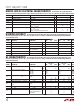
DYNAMIC ACCURACY
The l denotes the specifi cations which apply over the full operating temperature range,
otherwise specifi cations are at T
A
= 25°C. V
CC
= 2.7V, V
REF
= 2.5V, f
CLK
= f
CLK(MAX)
as defi ned in Recommended Operating Conditions,
unless otherwise noted.
SYMBOL PARAMETER CONDITIONS MIN
LTC1196
TYP MAX MIN
LTC1198
TYP MAX UNITS
S/(N + D) Signal-to-Noise Plus Distortion 190kHz/380kHz Input Signal 47/45 47/45 dB
THD Total Harmonic Distortion 190kHz/380kHz Input Signal 49/47 49/47 dB
Peak Harmonic or Spurious Noise 190kHz/380kHz Input Signal 53/46 53/46 dB
IMD Intermodulation Distortion f
IN1
= 189.37kHz
f
IN2
= 192.446kHz
51 51 dB
Full-Power Bandwidth 5 5 MHz
Full Linear Bandwidth [S/(N + D) > 44dB 0.5 0.5 MHz
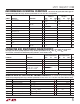
AC CHARACTERISTICS
The l denotes the specifi cations which apply over the full operating temperature range,
otherwise specifi cations are at T
A
= 25°C. V
CC
= 2.7V, V
REF
= 2.5V, f
CLK
= f
CLK(MAX)
as defi ned in Recommended Operating Conditions,
unless otherwise noted.
SYMBOL PARAMETER CONDITIONS MIN
LTC1196-1
LTC1198-1
TYP MAX MIN
LTC1196-2
LTC1198-2
TYP MAX UNITS
t
CONV
Conversion Time (See Figures 1, 2)
l
1.58
1.85
2.13
2.84
μs
μs
f
SMPL(MAX)
Maximum Sampling Frequency LTC1196
LTC1196
LTC1198
LTC1198
l
l
450
383
337
287
333
250
250
187
kHz
kHz
kHz
kHz
t
dDO
Delay Time, CLK↑ to D
OUT
Data Valid
C
LOAD
= 20pF
l
100 150
180
130 200
250
ns
ns
t
DIS
Delay Time CS↑ to D
OUT
Hi-Z
l
110 220 120 250 ns
t
en
Delay Time, CLK↓ to D
OUT
Enabled
C
LOAD
= 20pF
l
80 130 100 200 ns
t
hDO
Time Output Data Remains Valid After
CLK↑
C
LOAD
= 20pF
l
45 90 45 120 ns
t
f
D
OUT
Fall Time C
LOAD
= 20pF
l
10 30 15 40 ns
t
r
D
OUT
Rise C
LOAD
= 20pF
l
10 30 15 40 ns
C
IN
Input Capacitance Analog Input On Channel
Analog Input Off Channel
Digital Input
30
5
5
30
5
5
pF
pF
pF
Note 1: Stresses beyond those listed under Absolute Maximum Ratings
may cause permanent damage to the device. Exposure to any Absolute
Maximum Rating condition for extended periods may affect device
reliability and lifetime.