
Datasheet

LTC1257
3
1257fc
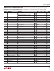
ELECTRICAL CHARACTERISTICS
The l denotes the specifications which apply over the full operating
temperature range, otherwise specifications are at T
A
= T
MIN
to T
MAX
. V
CC
= 4.75V to 15.75V, internal or external reference
(2.475V ≤ V
REF
≤ V
CC
– 2.7V), unless otherwise noted.
SYMBOL PARAMETER CONDITIONS MIN TYP MAX UNITS
OFF Offset Error When Using Internal Reference, LTC1257C
When Using Internal Reference, LTC1257I
l
l
±8
±10
LSB
LSB
When Using External Reference, LTC1257C
When Using External Reference, LTC1257I
l
l
±4
±5
mV
mV
OFF
TC
Offset Error Tempco When Using Internal Reference (Note 2)
When Using External Reference (Note 2)
l
l
±0.02
±15
±0.066
±30
LSB/°C
µV/°C
Gain Error
l
0.5 ±2 LSB
Gain Error Tempco (Note
2)
l
±0.01 ±0.02 LSB/°C
Reference
Reference Output Voltage I
REF
= 0, LTC1257C
I
RE
F = 0, LTC1257I
l
l
2.028
2.018
2.048 2.068
2.078
V
V
Reference Output Tempco I
REF
= 0
l
±0.06 LSB/°C
Reference Line Regulation I
REF
= 0, LTC1257C
I
REF
= 0, LTC1257I
l
l
±0.4
±0.7
LSB/V
LSB/V
Reference Load Regulation 0µA ≤ I
REF
≤ 100µA
l
±1 LSB
Reference Input Range V
CC
> V
REF
+ 2.7V
l
2.475 12 V
Reference Input Resistance
l
8 14 18 kΩ
Reference Input Capacitance (Note 2)
15 pF
Short-Circuit Current V
REF
Shorted to GND
l
90 mA
Power Supply
V
CC
Positive Supply Voltage For Specified Performance
l
4.75 15.75 V
I
CC
Supply Current 4.75V ≤ V
CC
≤ 5.25V
4.75V ≤ V
CC
≤ 15.75V
l
l
350
800
600
1500
µA
µA
Op Amp DC Performance
Short-Circuit Current Low V
OUT
Shorted to GND
l
60 mA
Short-Circuit Current High V
OUT
Shorted to V
CC
l
60 mA
Output Impedance to GND Input Code = 0
l
250 500 Ω
AC Performance
Voltage
Output Slew Rate 5kΩ in Parallel with 100pF
l
1.0 V/µs
Voltage Output Settling Time To ±1/2LSB, 5kΩ in Parallel with 100pF, V
CC
= 4.75V 6 µs
Digital Feedthrough (Notes 2, 3) 50 nV/s
Digital I/O
V
IH
Digital Input High Voltage
l
2.4 V
V
IL
Digital Input Low Voltage
l
0.8 V
V
OH
Digital Output High Voltage I
OUT
= –1mA, D
OUT
Only
l
V
CC
– 1 V
V
OL
Digital Output Low Voltage I
OUT
= 1mA, D
OUT
Only
l
0.4 V
I
LEAK
Digital Input Leakage V
IN
= GND to V
CC
l
±10 µA
C
IN
Digital Input Capacitance (Note 2)
l
10 pF
Switching (Note 2)
t
1
D
IN
Valid to CLK Setup
l
100 ns
t
2
D
IN
Valid to CLK Hold
l
25 ns
t
3
CLK High Time
l
350 ns
t
4
CLK Low Time
l
350 ns