
Datasheet
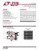

LTC1257
5
1257fc
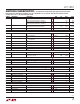
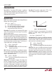
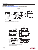
TYPICAL PERFORMANCE CHARACTERISTICS
Differential Nonlinearity (DNL)
Reference Compensation
Resistance vs C
L
Broadband Noise
Full-Scale Voltage
vs Temperature
Zero-Scale Voltage
vs Temperature Integral Nonlinearity (INL)
TEMPERATURE (°C)
–50
FULL-SCALE VOLTAGE (V)
2.0495
2.0490
2.0485
2.0480
2.0475
2.0470
2.0465
25 75
1257 G07
–25 0
50 100 125
V
CC
= 5V
INTERNAL REFERENCE
TEMPERATURE (°C)
–50 –25 25 50
ZERO-SCALE VOLTAGE (mV)
75 100
0.9
0.8
0.7
0.6
0.5
0.4
0.3
0.2
0.1
0
1257 G08
0 125
V
CC
= 5V
INTERNAL REFERENCE
CODE
0
ERROR (LSB)
2.0
1.6
1.2
0.8
0.4
0
–0.4
–0.8
–1.2
–1.6
–2.0
1024
2048
2560
1257 G09
512 1536
3072
3584
4096
V
CC
= 5V
INTERNAL REFERENCE
T
A
= 25°C
CODE
0
DNL ERROR (LSBs)
0.5
0.0
–0.5
1024 2048 2560
1257 TA05
512 1536 3072 3584
4098
C
L
(µF)
0.01
REFERENCE COMPENSATION RESISTANCE (Ω)
70
60
50
40
30
20
10
0
0.1 1
1257 G11
10 100
TIME = 5ms/DIV
0.1V/DIV
1257 G12
CODE = FFF
H
BW = 3Hz TO 1MHz
GAIN = 1100×
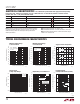
PIN FUNCTIONS
CLK (Pin 1): The TTL level input for the serial interface clock.
D
IN
(Pin 2): The TTL level input for the serial interface
data. Data on the D
IN
pin is latched into the shift register
on the rising edge of the serial clock.
LOAD (Pin 3): The TTL level input for the serial interface
load control. Data is loaded from the shift register into the
DAC
register, thus updating the DAC output when LOAD
is pulled low. The DAC register is transparent as long as
LOAD is held low.
D
OUT
(Pin 4): The output of the shift register which becomes
valid on the rising edge of the serial clock. The D
OUT
pin
is driven from GND to V
CC
by an internal CMOS inverter.
Multiple LTC1257s may be cascaded by connecting the
D
OUT
pin to the D
IN
pin of the next chip.
GND (Pin 5): Ground.
REF (Pin 6): The output of the 2.048V reference and the
input to the DAC resistor ladder. An external reference
with voltage from 2.475V to V
CC
– 2.7V may be used to
override the internal reference.