
Datasheet

LTC1257
8
1257fc
TYPICAL APPLICATIONS
OPERATION
Serial Interface
The data on the D
IN
input is loaded into the shift register
on the rising edge of the clock. The MSB is loaded first
and the LSB last. The DAC register loads the data from
the shift register when LOAD is pulled low, and remains
transparent until LOAD is pulled high and the data is latched.
An internal 5V regulator provides the supply
for the digital
logic. By limiting the internal digital signal swings to 5V,
digital noise is reduced. The buffered output of the 12-bit
shift register is available on the D
OUT
pin which will swing
from GND to V
CC
.
Multiple LTC1257s may be daisy chained together by
connecting the D
OUT
pin to the D
IN
pin of the next chip,
while the clock and load signals
remain common to all
chips in the daisy chain. The serial data is clocked to all
of the chips, then the LOAD signal is pulled low to update
all of them simultaneously. The maximum clocking rate
is 1.4MHz.
Reference
The LTC1257 includes an internal 2.048V reference, mak-
ing 1LSB equal to 500µV. The internal reference output
is turned off when the pin is forced above the reference
voltage, allowing an external reference to be connected to
the reference pin. The external reference must be greater
than 2.475V and less than V
CC
– 2.7V, and be capable of
driving the 10k minimum DAC resistor ladder.
If the reference output is driving a large capacitive load, a
series resistor must be added to insure stability. For any
capacitive load greater than 1µF, a 10Ω series resistor
will suffice
.
Voltage Output
The LTC1257 voltage output is able to pull within 2.7V of
V
CC
while sourcing 2mA. A internal NMOS transistor with
a 200Ω equivalent impedance pulls the output to ground.
The output is protected against short circuits and is able
to drive up to a 500pF capacitive load without oscillation.
If digital noise on the output causes a problem, a simple
100Ω, 0.1µF RC circuit can be
used to filter the noise.
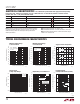
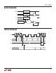
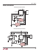
DAC with External Reference Filtering V
REF
and V
OUT
µP
15V
0.1µF
CONTROL OUTPUT
V
CC
V
REF
GND
V
OUT
D
IN
CLK
LOAD
D
OUT
LTC1257
1257 TA03
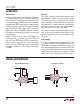
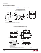
IN
OUT
GND
LT1021-10
0.1µF
0.1µF
1µF
V
CC
V
CC
V
REF
GND
V
OUT
V
OUT
D
IN
CLK
LOAD
D
OUT
LTC1257
1257 TA06
10Ω
5%
100Ω
5%