
Datasheet


11
LTC1264
1264fb
U
S
A
O
PP
L
IC
AT
I
WU
U
I FOR ATIO
For example, for an LTC1264 bandpass filter with f
CENTER
= 100kHz and f
CLK
= 2MHz, a 3.9MHz, 10mV input will
produce a 100kHz, 10mV output. A 1st or 2nd order
prefilter will reduce aliasing to acceptable levels in most
cases.
A GUIDE TO BANDPASS DESIGN
Filter design tools like FCAD require design specification
inputs such as passband ripple, attenuation, passband
width and stopband width in order to calculate filter
parameters f
O
, Q, f
n
or poles and zeroes. The results of
these filter approximations most often require Q values
which make excessive demands on the gain-bandwidth
products of active filter realizations. The active filter de-
signer should define a gain response so that the filter’s
mathematical approximation has practical requirements.
Table 4 is a guide to practical design specifications for
realizing bandpass filters with LTC1264 (please also refer
to the Typical Maximum Q vs Clock Frequency and Band-
pass Gain Error graphs under Typical Performance Char-
acteristics).
A Bandpass Design Example
Filter Type: Bandpass
Filter Response: Butterworth
Passband Ripple: 3dB
Attenuation: 60dB
Center Frequency: 40kHz (f
CENTER
)
Passband Width: 10kHz
Stopband Width: 60kHz
Implementing the Bandpass Design
With the LTC1264 in Mode 1b, Butterworth and Chebyshev
bandpass designs with f
CLK
to f
CENTER
ratios greater than
20:1 are possible.
First choose the clock frequency which in Mode 1b must
be greater than 20 times the bandpass center frequency of
40kHz. For this example, let’s choose f
CLK
to be 1MHz.
Table 6 lists the resistors for for the bandpass design
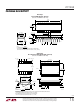
example and Figure 11 shows the complete circuit.
Table 4. Bandpass Design Specifications (f
CENTER
is center
frequency of passband.)
PASSBAND PASSBAND STOPBAND ATTENU-
RIPPLE WIDTH WIDTH ATION
(dB) (Hz) (Hz) (dB)
≤ 3dB for Butterworth ≥ f
CENTER
/20 ≥ 5 × Passband –40 to –60
≤0.1 for Chebyshev ≥ f
CENTER
/20 ≥ 5 × Passband –40 to –60
Note: Reducing passband ripple or attenuation will decrease Q values. The
filter order may also increase.
Table 5. Calculated Filter Parameters
STAGE f
O
Q
1 38.1201kHz 4.3346
2 41.9726kHz 4.3346
3 35.6418kHz 10.5221
4 44.8911kHz 10.5221
Table 6. Calculated Mode 1b Resistors to Nearest 1% Value
Using Table 5 Filter Parameters and Figure 10 Equations
STAGE R1 R2 R3 R5 R6
1 52.3k 10k 56.2k 5k 6.98k
2 47.5k 10k 51.1k 5k 11.8k
3 56.2k 10k 147k 5k 5.11k
4 44.2k 10k 118k 5k 20.5k
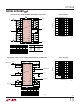
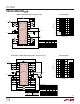
Figure 10. Equations for Resistors in Mode 1b Operation
R2 = 10k
R5 = 5k
f
i
=
R1 = (FOR BANDPASS)
R6 =
H
OBP
= + 1
R3 =
R3
H
OBP
R5•f
O
2
f
i
2
–
f
O
2
()
√
()
Q
2
f
O
f
CENTER
–
f
CENTER
f
O
()
2
R2•Q
R6
R6 + 5
()
√
1264 F10
f
CLK
20