
Datasheet

19
LTC1273
LTC1275/LTC1276
127356fa
U
S
A
O
PP
L
IC
AT
I
WU
U
I FOR ATIO
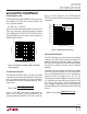
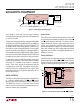
TMS320C25
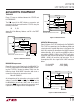
Figure 17 shows an interface between the LTC1273 and
the TMS320C25.
The W/R signal of the DSP initiates a conversion and
conversion results are read from the LTC1273 using the
following instruction:
IN D, PA
where D is Data Memory Address and PA is the PORT
ADDRESS.
Figure 17. TMS320C25 Interface
DATA BUS
LTC1273/75/76 • F17
ADDRESS BUS
D0
D16
R/W
READY
IS
A1
A16
TMS320C25
ADDRESS
DECODE
EN
D0/8
D11
RD
BUSY
CS
HBEN
LTC1273/75/76
ADDITIONAL PINS OMITTED FOR CLARITY
DATA BUS
LTC1273/75/76 • F18
ADDRESS BUS
D0
D11
R/W
DTACK
AS
A1
A23
MC68000
ADDRESS
DECODE
EN
D0/8
D11
RD
BUSY
CS
HBEN
LTC1273/75/76
ADDITIONAL PINS OMITTED FOR CLARITY
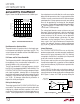
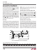
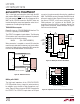
Figure 18. MC68000 Interface
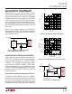
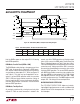
8085A/Z80 Microprocessor
Figure 19 shows an LTC1273 interface for the Z80/8085A.
The LTC1273 is operating in the Slow Memory Mode and
a two byte read is required. Not shown in the figure is the
8-bit latch required to demultiplex the 8085A common
address/data bus. A0 is used to assert HBEN so that an
even address (HBEN = LOW) to the LTC1273 will start a
conversion and read the low data byte. An odd address
(HBEN = HIGH) will read the high data byte. This is
accomplished with the single 16-bit LOAD instruction
below.
For the 8085A LHLD (B000)
For the Z80 LDHL, (B000)
Figure 19. 8085A and Z80 Interface
DATA BUS
LTC1273/75/76 • F19
ADDRESS BUS
D0
D7
RD
WAIT
MREQ
A0
A15
Z80
8085A
ADDRESS
DECODE
EN
D0/8
D7
RD
BUSY
CS
HBEN
ADDITIONAL PINS OMITTED FOR CLARITY
LTC1273/75/76
A0
MC68000 Microprocessor
Figure 18 shows a typical interface for the MC68000. The
LTC1273 is operating in the Slow Memory Mode. Assum-
ing the LTC1273 is located at address C000, then the
following single 16-bit MOVE instruction both starts a
conversion and reads the conversion result:
Move.W $C000,D0
At the beginning of the instruction cycle when the ADC
address is selected, BUSY and CS assert DTACK so that
the MC68000 is forced into a WAIT state. At the end of
conversion, BUSY returns high and the conversion result
is placed in the D0 register of the microprocessor.