
Datasheet


12
LTC1273
LTC1275/LTC1276
127356fa
U
S
A
O
PP
L
IC
AT
I
WU
U
I FOR ATIO
Figure 5 shows the IMD performance at a 30kHz input.
FREQUENCY (kHz)
0
–120
AMPLITUDE (dB)
–100
–80
–60
–40
40 80
120
160
LTC1273/75/76 • F05
–20
0
20 60 100
140
f
SAMPLE
= 300kHz
f
IN1
= 29.37kHz
f
IN2
= 32.446kHz
Figure 5. Intermodulation Distortion Plot
the analog input must settle after the small current spike
before the next conversion starts. Any op amp that settles
in 600ns to small current transients will allow maximum
speed operation. If slower op amps are used, more settling
time can be provided by increasing the time between
conversions. Suitable devices capable of driving the ADCs’
A
IN
input include the LT1190/LT1191, LT1007, LT1220,
LT1223 and LT1224 op amps.
The analog input tolerates source resistance very well.
Here again, the only requirement is that the analog input
must settle before the next conversion starts. For larger
source resistance, full DC accuracy can be obtained if
more time is allowed between conversions. For more
information, see the Acquisition Time vs Source Resis-
tance curve in the Typical Performance Characteristics
section. For optimum frequency domain performance
[e.g., S/(N + D)], keep the source resistance below 100Ω.
Internal Reference
The LTC1273/LTC1275/LTC1276 have an on-chip, tem-
perature compensated, curvature corrected, bandgap ref-
erence which is factory trimmed to 2.42V. It is internally
connected to the DAC and is available at pin 2 to provide
up to 1mA current to an external load.
For minimum code transition noise the reference output
should be decoupled with a capacitor to filter wideband
noise from the reference (10µF tantalum in parallel with a
0.1µF ceramic).
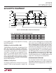
I
n the LTC1275, the V
REF
pin can be driven above its
normal value with a DAC or other means to provide input
span adjustment or to improve the reference temperature
drift. Figure 6 shows an LT1006 op amp driving the
V
REF(OUT)
≥ 2.45V
3Ω
INPUT RANGE
±1.033V
REF(OUT)
–
+
LT1006
LTC1275
A
IN
AGND
V
REF
10µF
LTC1273/75/76 • F06
Figure 6. Driving the V
REF
with the LT1006 Op Amp
Peak Harmonic or Spurious Noise
The peak harmonic or spurious noise is the largest spec-
tral component excluding the input signal and DC. This
value is expressed in decibels relative to the RMS value of
a full scale input signal.
Full Power and Full Linear Bandwidth
The full power bandwidth is that input frequency at which
the amplitude of the reconstructed fundamental is re-
duced by 3dB for a full scale input signal.
The full linear bandwidth is the input frequency at which
the S/(N + D) has dropped to 68dB (11 effective bits). The
LTC1273/LTC1275/LTC1276 have been designed to opti-
mize input bandwidth, allowing ADCs to undersample
input signals with frequencies above the converters’ Nyquist
Frequency. The noise floor stays very low at high frequen-
cies; S/(N + D) becomes dominated by distortion at
frequencies far beyond Nyquist.
Driving the Analog Input
The analog inputs of the LTC1273/LTC1275/LTC1276 are
easy to drive. They draw only one small current spike while
charging the sample-and-hold capacitor at the end of
conversion. During conversion the analog input draws no
current. The only requirement is that the amplifier driving