
Datasheet


15
LTC1273
LTC1275/LTC1276
127356fa
U
S
A
O
PP
L
IC
AT
I
WU
U
I FOR ATIO
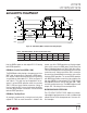
Figure 11. Power Supply Grounding Practice
LTC1273/75/76 • F11
A
IN
AGND V
REF
V
DD
DGND
LTC1273
DIGITAL
SYSTEM
0.1µF
+
–
ANALOG GROUND PLANE
GROUND CONNECTION
TO DIGITAL CIRCUITRY
ANALOG
INPUT
CIRCUITRY
3 2 24 12
1
0.1µF
10µF10µF
error voltage in series with the input signal, attention
should be paid to reducing the ground circuit impedances
as much as possible.
A single point analog ground plane separate from the logic
system ground should be established at Pin 3 (AGND) or
as close as possible to the ADC, as shown in Figure 11. Pin
12 (DGND) and all other analog grounds should be con-
nected to this single analog ground point. No other digital
grounds should be connected to this analog ground point.
Low impedance analog and digital power supply common
returns are essential to low noise operation of the ADC and
the width for these traces should be as wide as possible.
In applications where the ADC data outputs and control
signals are connected to a continuously active micropro-
cessor bus, it is possible to get errors in conversion
results. These errors are due to feedthrough from the
microprocessor to the ADC. The problem can be elimi-
nated by forcing the microprocessor into a WAIT state
during conversion or by using three-state buffers to iso-
late the ADC data bus.
DIGITAL INTERFACE
The ADCs are designed to interface with microprocessors
as a memory mapped device. The CS and RD control
inputs are common to all peripheral memory interfacing.
The HBEN input serves as a data byte select for 8-bit
processors and is normally either connected to the micro-
processor address bus or grounded.
Internal Clock
These ADCs have an internal clock that eliminates the need
for synchronization between an external clock and the CS
and RD signals found in other ADCs. The internal clock is
factory trimmed to achieve a typical conversion time of
2.45µs, and a maximum conversion time over the full
operating temperature range of 2.7µs. No external adjust-
ments are required and, with the guaranteed maximum
acquisition time of 600ns, throughput performance of
300ksps is assured.
Timing and Control
Conversion start and data read operations are controlled
by three digital inputs: HBEN, CS and RD. Figure 12 shows
the logic structure associated with these inputs. The three
signals are internally gated so that a logic “0” is required
CONVERSION
START (RISING
EDGE TRIGGER)
LTC1273/75/76 • F12
BUSY
FLIP
FLOP
CLEAR
QD
19
21
20
ACTIVE HIGH
ACTIVE HIGH
ENABLE THREE-STATE OUTPUTS
D11....D0/8 = DB11....DB0
ENABLE THREE-STATE OUTPUTS
D11....D8 = DB11....DB8
D7....D4 = LOW
D3/11....D0/8 = DB11....DB8
HBEN
CS
RD
LTC1273/75/76
D11....D0/8 ARE THE ADC DATA OUTPUT PINS
DB11....DB0 ARE THE 12-BIT CONVERSION RESULTS
*
Figure 12. Internal Logic for Control Inputs CS, RD and HBEN