
Datasheet


17
LTC1274/LTC1277
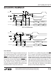
In slow memory mode the processor applies a logic low to
RD (= CONVST), starting the conversion. BUSY goes low,
forcing the processor into a Wait state. The previous
conversion result appears on the data outputs. When the
conversion is complete, the new conversion results ap-
pear on the data outputs; BUSY goes high releasing the
processor; the processor applies a logic high to RD
(= CONVST) and reads the new conversion data.
In ROM mode the processor applies a logic low to RD
(= CONVST), starting a conversion and reading the
previous conversion result. After the conversion is com-
plete, the processor can read the new result and initiate
another conversion.
The narrow logic pulse on CONVST ensures that CONVST
doesn’t return high during the conversion (see Note 13
following the Timing Characteristics table).
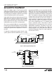
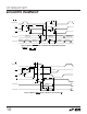
In Mode 2 (Figure 15) CS is tied low. The falling edge of
CONVST signal again starts the conversion. Data outputs
both are in three-state until read by the MPU with the RD
signal. Mode 2 can be used for operation with a shared
MPU databus.
In slow memory and ROM modes (Figures 16 and 17) CS
is tied low and CONVST and RD are tied together. The MPU
starts the conversion and reads the output with the RD
signal. Conversions are started by the MPU or DSP (no
external sample clock).
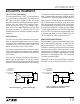
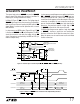
DATA (N – 1)
DB11 TO DB0
DATA (N – 1)
DB7 TO DB0
CONVST
BUSY
LTC1274/77 • F13
t
16
t
15
t
4
t
5
t
6
CS = RD = 0
HBEN (LTC1277)
DATA N
DB11 TO DB0
DATA N
DB7 TO DB0
DATA N
DB11 TO DB8
DATA N
DB7 TO DB0
DATA (N + 1)
DB11 TO DB0
DATA (N + 1)
DB7 TO DB0
LTC1274 DATA
LTC1277 DATA
t
7
t
CONV
(SAMPLE N) (SAMPLE N + 1)
(CONVST = )
Figure 13. Mode 1a. CONVST Starts a Conversion. Data Outputs Always Enabled
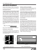
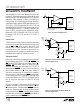
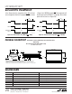
U
S
A
O
PP
L
IC
AT
I
WU
U
I FOR ATIO
CONVERSION
START (RISING
EDGE TRIGGER)
1274/77 • F12
BUSY
FLIP
FLOP
CLEAR
QD
ACTIVE HIGH
ENABLE THREE-STATE OUTPUTS
DB11....DB0
CS
RD
CONVST
NAP
SLEEP
Figure 12. Internal Logic for Control Inputs CS, RD, CONVST, NAP and SLEEP (LTC1277)