
Datasheet


8
LTC1278
CONVERSION DETAILS
The LTC1278 uses a successive approximation algorithm
and an internal sample-and-hold circuit to convert an
analog signal to a 12-bit parallel output. The ADC is
complete with a precision reference and an internal clock.
The control logic provides easy interface to microproces-
sors and DSPs. (Please refer to the Digital Interface
section for the data format.)
Conversion start is controlled by the CS and CONVST
inputs. At the start of conversion the successive approxi-
mation register (SAR) is reset. Once a conversion cycle
has begun it cannot be restarted.
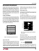
During conversion, the internal 12-bit capacitive DAC
output is sequenced by the SAR from the most significant
bit (MSB) to the least significant bit (LSB). Referring to
Figure 1, the A
IN
input connects to the sample-and-hold
capacitor during the acquire phase, and the comparator
TEST CIRCUITS
Load Circuits for Output Float DelayLoad Circuits for Access Timing
3k C
L
DBN
DGND
A) HIGH-Z TO V
OH
(t
8
)
AND V
OL
TO V
OH
(t
6
)
C
L
DBN
3k
5V
B) HIGH-Z TO V
OL
(t
8
)
AND V
OH
TO V
OL
(t
6
)
DGND
LTC1278 TA08
3k 10pF
DBN
DGND
A) V
OH
TO HIGH-Z
10pF
DBN
3k
5V
B) V
OL
TO HIGH-Z
DGND
1278 • TA08
SHDN to CONVST Wake-Up Timing
t
3
SHDN
CONVST
LTC1278 • TC03
APPLICATIONS INFORMATION
WUU
U
offset is nulled by the feedback switch. In this acquire
phase, a minimum delay of 200ns will provide enough
time for the sample-and-hold capacitor to acquire the
analog signal. During the convert phase, the comparator
feedback switch opens, putting the comparator into the
V
DAC
LTC1278 F1
+
–
C
DAC
DAC
SAMPLE
HOLD
C
SAMPLE
S
A
R
12-BIT
LATCH
COMPARATOR
SAMPLE
SI
A
IN
Figure 1. A
IN
Input
CS to RD Setup Timing
t
1
CS
RD
LTC1278 • TC01
CS to CONVST Setup Timing
t
2
CS
CONVST
LTC1278 • TC02
TI I G DIAGRA S
WU W