
Datasheet


11
LTC1292/LTC1297
12927fb
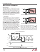
on two port lines and the D
OUT
signal is read on a third port
line. After a falling CLK edge each data bit is loaded into the
carry bit and then rotated into the accumulator. Once the
first 8 MSBs have been shifted into the accumulator they
are loaded into register R2. The last four bits are shifted in
the same way and loaded into register R3. The output data
is left-justified in registers R2 and R3 (Figure 5).
For the LTC1297 four NOPs need to be inserted in the 8051
code after CS goes low to allow the LTC1297 to wake up
from power shutdown (t
suCS
).
U
S
A
O
PP
L
IC
AT
I
WU
U
I FOR ATIO
LABEL MNEMONIC OPERAND COMMENTS
LDAA #$50 CONFIGURATION DATA FOR SPCR
STAA $1028 LOAD DATA INTO SPCR ($1028)
LDAA #$1B CONFIG. DATA FOR PORT D DDR
STAA $1009 LOAD DATA INTO PORT D DDR
LDAA #$00 LOAD DUMMY DIN WORD INTO
ACC A
STAA $50 LOAD DUMMY DIN DATA INTO $0
LOOP LDX #$1000 LOAD INDEX REGISTER X WITH
$1000
LDAB #$00 LOAD ACC B WITH $00
LDAA $50 LOAD DIN INTO ACC FROM $50
BCLR $08,X,$01 D0 GOES LOW (CS GOES LOW)
NOP 3 NOP FOR t
suCS
TIMING
NOP
NOP
STAA $102A LOAD DUMMY DIN INTO SPI,
START CLK
LABEL MNEMONIC OPERAND COMMENTS
MC68HC11 CODE for LTC1297 Interface
LOOP1 LDAA $1029 CHECK SPI STATUS REG
BPL LOOP1 CHECK IF TRANSFER IS DONE
LDAA $102A LOAD LTC1297 MSBs INTO ACC A
STAA $61 STORE MSBs IN $61
STAA $102A LOAD DUMMY DIN INTO SPI,
START SCK
LOOP2 LDAA $1029 CHECK SPI STATUS RES
BPL LOOP2 CHECK IF TRANSFER IS DONE
BSET $08X,$01 D0 GOES HIGH (CS GOES HIGH)
LDAA $102A LOAD LTC1297 LSBs INTO ACC A
STAA $62 STORE LSBs IN $62
ROR $61 ROTATE RIGHT WITH CARRY
ROR $62 NEEDED TO RIGHT JUSTIFY
ROR $61 THE DATA IN $61 AND $62
ROR $62
JMP LOOP START NEXT CONVERSION
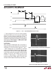
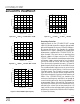
BYTE 2
B3B7
B6
B5
B4 B2
B0
B1
B10 B9 B8B11
OO
OO
BYTE 1
D
OUT
FROM LTC1297 STORED ON MC68HC11 RAM
LOCATION #61
LOCATION #62
MSB
LTC1292/7 F04
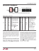
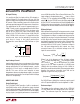
CLK
D
OUT
LTC1297
CS
ANALOG
INPUTS
DO
SCK
MISO
MC68HC11
Figure 4. Hardware and Software Interface to Motorola MC68HC11 Microcontroller
The data is right- justified in the two memory locations by
rotating right twice (Figure 4). ANDing the first byte with
0F
HEX
clears the four most significant bits. This operation
was not included in the code. It can be inserted in the data
gathering loop or outside the loop when the data is
processed.
Interfacing to the Parallel Port of the Intel 8051 Family
The Intel 8051 has been chosen to show the interface
between the LTC1292/LTC1297 and parallel port
microprocessors. The signals CS and CLK are generated