
Datasheet


2
LTC1334
A
U
G
W
A
W
U
W
ARB
S
O
LU
T
EXI T
I
S
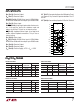
ORDER PART
NUMBER
LTC1334CG
LTC1334CNW
LTC1334CSW
LTC1334IG
LTC1334ISW
(Note 1)
Supply Voltage (V
CC
) ............................................. 6.5V
Input Voltage
Drivers ................................... –0.3V to (V
CC
+ 0.3V)
Receivers ............................................. –25V to 25V
ON/OFF, LB, SEL1, SEL2 ........ –0.3V to (V
CC
+ 0.3V)
Output Voltage
Drivers ................................................. –18V to 18V
Receivers ............................... –0.3V to (V
CC
+ 0.3V)
Short-Circuit Duration
Output ........................................................ Indefinite
V
DD
, V
EE
, C1
+
, C1
–
, C2
+
, C2
–
.......................... 30 sec
Operating Temperature Range
Commercial........................................... 0°C to 70°C
Industrial............................................ –40°C to 85°C
Storage Temperature Range ................ –65°C to 150°C
Lead Temperature (Soldering, 10 sec)................ 300°C
WU
U
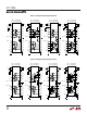
PACKAGE
/
O
RDER I FOR ATIO
T
JMAX
= 125°C, θ
JA
= 90°C/W (G)
T
JMAX
= 125°C, θ
JA
= 56°C/W (NW)
T
JMAX
= 125°C, θ
JA
= 85°C/W (SW)
1
2
3
4
5
6
7
8
9
10
11
12
13
14
TOP VIEW
28
27
26
25
24
23
22
21
20
19
18
17
16
15
C2
+
C2
–
V
CC
R
B1
R
A1
D
Z1
/DE1
D
Y1
LB
ON/OFF
D
Y2
D
Z2
/DE2
R
A2
R
B2
V
EE
C1
+
C1
–
V
DD
A1
B1
Y1
Z1
SEL1
SEL2
Z2
Y2
B2
A2
GND
SW PACKAGE
28-LEAD PLASTIC SO WIDE
G PACKAGE
28-LEAD PLASTIC SSOP
NW PACKAGE
28-LEAD PDIP WIDE
Consult factory for Military grade parts.
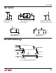
DC ELECTRICAL CHARACTERISTICS
SYMBOL PARAMETER CONDITIONS MIN TYP MAX UNITS
RS485 Driver (SEL1 = SEL2 = High)
V
OD1
Differential Driver Output Voltage (Unloaded) I
O
= 0 ● 6V
V
OD2
Differential Driver Output Voltage (With Load) Figure 1, R = 50Ω (RS422) ● 2.0 6 V
Figure 1, R = 27Ω (RS485) ● 1.5 6 V
∆V
OD
Change in Magnitude of Driver Differential Figure 1, R = 27Ω or R = 50Ω ● 0.2 V
Output Voltage for Complementary Output States
V
OC
Driver Common Mode Output Voltage Figure 1, R = 27Ω or R = 50Ω ● 3V
∆V
OC
Change in Magnitude of Driver Common Mode Figure 1, R = 27Ω or R = 50Ω ● 0.2 V
Output Voltage for Complementary Output States
I
OSD
Driver Short-Circuit Current –7V ≤ V
O
≤ 12V, V
O
= High ● 35 250 mA
–7V ≤ V
O
≤ 12V, V
O
= Low (Note 4) ● 10 250 mA
I
OZD
Three-State Output Current (Y, Z) –7V ≤ V
O
≤ 12V ● ±5 ±500 µA
RS232 Driver (SEL1 = SEL2 = Low)
V
O
Output Voltage Swing Figure 4, R
L
= 3k, Positive ● 5 6.5 V
Figure 4, R
L
= 3k, Negative ● –5 –6.5 V
I
OSD
Output Short-Circuit Current V
O
= 0V ● ±60 mA
Driver Inputs and Control Inputs
V
IH
Input High Voltage D, DE, ON/OFF, SEL1, SEL2, LB ● 2V
V
IL
Input Low Voltage D, DE, ON/OFF, SEL1, SEL2, LB ● 0.8 V
I
IN
Input Current D, SEL1, SEL2 ● ±10 µA
DE, ON/OFF, LB
● –4 –15 µA
The ● denotes specifications which apply over the full operating
temperature range, otherwise specifications are at T
A
= 25°C. V
CC
= 5V, C1 = C2 = C3 = C4 = 0.1µF (Notes 2, 3)