
Datasheet


7
LTC1334
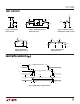
PI FU CTIO S
U
UU
R
B2
(Pin 16): Receiver Output.
R
A2
(Pin 17): Receiver Output.
D
Z2
/DE2 (Pin 18): RS232 Driver Input in RS232 Mode.
RS485 Driver Enable with internal pull-up in RS485 mode.
D
Y2
(Pin 19): Driver Input.
ON/OFF (Pin 20): A high logic input enables the transceiv-
ers. A low puts the device into shutdown mode and
reduces I
CC
to 10µA. This pin has an internal pull-up.
LB (Pin 21): Loopback Control Input. A low logic level
enables internal loopback connections. This pin has an
internal pull-up.
D
Y1
(Pin 22): Driver Input.
D
Z1
/DE1 (Pin 23): RS232 Driver Input in RS232 Mode.
RS485 Driver Enable with internal pull-up in RS485 mode.
R
A1
(Pin 24): Receiver Output.
R
B1
(Pin 25): Receiver Output.
V
CC
(Pin 26): Positive Supply; 4.75V ≤ V
CC
≤ 5.25V
C2
–
(Pin 27): Commutating Capacitor C2 Negative Termi-
nal. Requires 0.1µF external capacitor between Pins 27
and 28.
C2
+
(Pin 28): Commutating Capacitor C2 Positive Terminal.
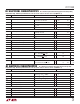
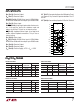
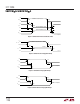
FU CTIO TABLES
UU
RS485 Driver Mode
INPUTS OUTPUTS
ON/OFF SEL DE D CONDITIONS Z Y
1 1 1 0 No Fault 0 1
1 1 1 1 No Fault 1 0
1 1 1 X Thermal Fault Z Z
110X X ZZ
01XX X ZZ
RS232 Driver Mode
INPUTS
OUTPUTS
ON/OFF SEL D CONDITIONS Y, Z
1 0 0 No Fault 1
1 0 1 No Fault 0
1 0 X Thermal Fault Z
00X X Z
RS485 Receiver Mode
INPUTS OUTPUTS
ON/OFF SEL B – A R
A
R
B
*
1 1 < –0.2V 0 1
1 1 > 0.2V 1 1
1 1 Inputs Open 1 1
01 XZZ
*See Note 5 of Electrical Characteristics table.
RS232 Receiver Mode
INPUTS
OUTPUTS
ON/OFF SEL A, B R
A
, R
B
10 0 1
10 1 0
1 0 Inputs Open 1
00 X Z
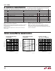
1 28
C2
+
C2
–
C1
+
V
EE
R
B2
R
A2
D
Z2
/DE2
D
Y2
ON/OFF
LB
D
Y1
D
Z1
/DE1
R
A1
R
B1
V
CC
14 15
13
12
11
10
9
8
7
6
5
4
3
2
16
17
18
19
20
21
22
23
24
25
26
27
GND
A2
B2
Y2
Z2
SEL2
SEL1
Z1
Y1
B1
A1
V
DD
C1
–