
Datasheet


4
LTC1337
1337fa
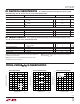
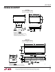
TYPICAL PERFOR A CE CHARACTERISTICS
UW
V
CC
Supply Current
TEMPERATURE (°C)
0
LEAKAGE CURRENT (µA)
60
45
40
35
30
25
20
15
10
5
0
1337 G05
20 7010
30
40
50
V
OUT
= –20V
V
OUT
= 20V
TEMPERATURE (°C)
0
SUPPLY CURRENT (mA)
60
20
16
14
12
10
8
6
4
2
0
1337 G04
20 7010
30
40
50
3 DRIVERS LOADED
R
L
= 3k
1 DRIVER LOADED
R
L
= 3k
Driver Short-Circuit Current
Driver Leakage in Shutdown
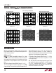
Receiver Short-Circuit Current Driver Output Waveforms
INPUT
DRIVER
OUTPUT
R
L
= 3k
DRIVER
OUTPUT
R
L
= 3k
C
L
= 2500pF
Receiver Output Waveforms
RX
OUTPUT
C
L
= 50pF
INPUT
TEMPERATURE (°C)
0
SHORT-CIRCUIT CURRENT (mA)
60
20
18
16
14
12
10
8
6
4
2
1337 G06
20 7010
30
40
50
I
SC
+
I
SC
–
TEMPERATURE (°C)
0
SHORT-CIRCUIT CURRENT (mA)
60
55
50
45
40
35
30
25
20
15
10
1337 G07
20 7010
30
40
50
I
SC
+
I
SC
–
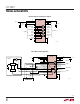
UU
U
PI FU CTIO S
V
CC
: 5V Input Supply Pin. Supply current less than 1µA in
the Shutdown mode. This pin should be decoupled with a
0.1µF ceramic capacitor.
GND: Ground Pin.
ON/OFF: TTL/CMOS Compatible Shutdown Pin. A logic
low puts the device in the Shutdown mode which reduces
input supply current to less than 1µA and places all drivers
and receivers in high impedance state. This pin cannot
float.
V
+
: Positive Supply Output (RS232 Drivers). V
+
≅ 2V
CC
–
1V. This pin requires an external capacitor C = 0.1µF for
charge storage. The capacitor may be tied to ground or 5V.
With multiple devices, the V
+
and V
–
pins may be paral-
leled into common capacitors. For large numbers of
devices, increasing the size of the shared common storage
capacitors is recommended to reduce ripple.
V
–
: Negative Supply Output (RS232 Drivers). V
–
≅ (2V
CC
–1.5V). This pin requires an external capacitor C = 0.1µF
for charge storage.
C1
+
, C1
–
, C2
+
, C2
–
: Commutating Capacitor Inputs. These
pins require two external capacitors C = 0.1µF. One from
C1
+
to C1
–
, and another from C2
+
to C2
–
. To maintain
charge pump efficiency, the capacitor’s effective series
resistance should be less than 50Ω.