
Datasheet

10
LTC1343
APPLICATIONS INFORMATION
WUU
U
will configure the port for DCE mode when high, and DTE
when low.
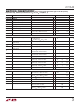
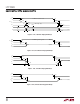
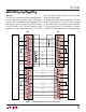
The interface protocol may be selected simply by plugging
the appropriate interface cable into the connector. The
mode pins are routed to the connector and are left uncon-
nected (1) or wired to ground (0) in the cable as shown in
Figure 11.
The pull-up resistors R1 through R4 will ensure a binary
1 when a pin is left unconnected and that the two LTC1343s
and the LTC1344 enter the no-cable mode when the cable
is removed. In the no-cable mode the LTC1343 supply
current drops to less than 200µA and all LTC1343 driver
outputs and LTC1344 resistive terminations are forced
into a high impedance state. Note that the data latch pin,
LATCH, is shorted to ground for all chips.
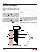
The interface protocol may also be selected by the serial
controller or host microprocessor as shown in Figure 12.
The mode selection pins M0, M1, M2 and DCE/DTE can be
shared between multiple interface ports, while each port
Figure 11: Single Port DCE/V.35 Mode Selection in the Cable
RL (Remote Loop-back) and RI (Ring Indicate). The
LTC1344 cable termination chip is used only for the clock
and data signals because they must support V.35 cable
termination. The control signals do not need any external
resistors.
Mode Selection
The interface protocol is selected using the mode select
pins M0, M1, M2 and CTRL/CLK (see the Mode Selection
table). The CTRL/CLK pin should be pulled high if the
LTC1343 is being used to generate control signals and
pulled low if used to generate clock and data signals.
For example, if the port is configured as a V.35 interface,
the mode selection pins should be M2 = 1, M1 = 0, M0 = 0.
For the control signals, CTRL/CLK = 1 and the drivers and
receivers will operate in RS232 (V.28) electrical mode. For
the clock and data signals, CTRL/CLK = 0 and the drivers
and receivers will operate in V.35 electrical mode, except
for the single-ended driver and receiver which will operate
in the RS232 (V.28) electrical mode. The DCE/DTE pin
NC
NC
CABLE
1343 F11
17
18
19
21
LTC1343
LTC1343
CONNECTOR
20
21
19
18
17
22
21
M2 M1
LTC1344
LATCH
M0 (DATA)
23 24 1
CTRL/CLK
22
(DATA)
M0
M1
M2
DCE/DTE
LATCH
20
CTRL/CLK
22
DCE/DTE
M2
M1
M0
(DATA)
LATCH
V
CC
DCE/
DTE
R1, 10k
V
CC
R2, 10k
V
CC
R3, 10k
V
CC
R4, 10k
V
CC