
Datasheet


17
LTC1343
No-Cable Mode
The no-cable mode (M0 = M1 = M2 = 1) is intended for the
case when the cable is disconnected from the connector.
The charge pump, bias circuitry, drivers and receivers are
turned off, the driver outputs are forced into a high
impedance state, and the supply current drops to less than
200µA. It can also be used to share I/O lines with other
drivers and receivers without loading down the signals.
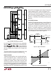
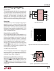
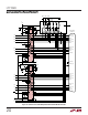
Charge Pump
The LTC1343 uses an internal capacitive charge pump to
generate V
DD
and V
EE
as shown in Figure 28. A voltage
doubler generates about 8V on V
DD
and a voltage inverter
generates about –7.5V for V
EE
. Four 1µF surface mounted
tantalum or ceramic capacitors are required for C1, C2, C3
and C4. The V
EE
capacitor C5 should be a minimum of
3.3µF. All capacitors are 16V.
Receiver Fail-Safe and Glitch Filter
All LTC1343 receivers feature fail-safe operation in all
modes except no-cable mode. If the receiver inputs are left
floating or shorted together by a termination resistor, the
receiver output will always be forced to a logic high.
External pull-up resistors are required on receiver outputs
if fail-safe operation in the no-cable mode is desired.
When the chip is configured for control signals by pulling
the CTRL/CLK pin high, a glitch filter is connected to all
receiver inputs. The filter will reject any glitches at the
receiver inputs less than 300ns.
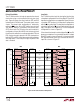
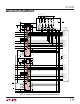
V.10 Driver Rise and Fall Times
The rise and fall times of the V.10 drivers is programmed
by placing a 1/8W, 5% resistor between the 423 SET (Pin
25) and ground. The graph of Driver Rise and Fall Times
vs Resistor Value is shown in Figure 29.
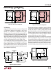
Enabling the Single-Ended Driver and Receiver
When the LTC1343 is being used to generate the control
signals (CTRL/CLK = high) and the EC pin is pulled low, the
DCE/DTE pin becomes an enable for driver 1 and receiver
4 so their inputs and outputs can be tied together as shown
in Figure 30.
APPLICATIONS INFORMATION
WUU
U
Figure 30. Single-Ended Driver and Receiver Enable
Figure 29. V.10 Driver Rise and Fall Time vs Resistor Value
Figure 28. Charge Pump
44
43
42
41
40
1343 F28
1
2
3
4
8
C3
1µF
C4
1µF
5V
C1
1µF
C2
1µF
C5
3.3µF
LTC1343
V
DD
C1
+
PWRV
CC
C1
–
V
CC
C2
+
C2
–
V
EE
PGND
GND
+
+
+
+
+
RESISTANCE (Ω)
DRIVER RISE/FALL TIME (µs)
1k
100
10
1
0.1
100k 1M 5M
1343 F29
10k
39
26
LTC1343
1343 F30
5
21
16
20
24
EC
D1
CTRL/CLK
DCE/DTE
R4
V
CC