
Datasheet

5
LTC1343
V
DD
(Pin 1): Generated Positive Supply Voltage for
RS232. Connect a 1µF capacitor to ground.
C1
+
(Pin 2): Capacitor C1 Positive Terminal. Connect a
1µF capacitor between C1
+
and C1
–
.
PWRV
CC
(Pin 3): Positive Supply for the Charge Pump.
4.75V ≤ PWRV
CC
≤ 5.25V. Tie to V
CC
(Pin 8) and bypass
with a 1µF capacitor to ground.
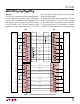
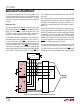
PIN FUNCTIONS
UUU
C1
–
␣ (Pin 4): Capacitor C1 Negative Terminal.
D1 (Pin 5): TTL Level Driver 1 Input.
D2 (Pin 6): TTL Level Driver 2 Input.
D3 (Pin 7): TTL Level Driver 3 Input. Becomes a CMOS
level output when the chip is in the echoed clock mode
(EC = 0V).
Note 1: Absolute Maximum Ratings are those beyond which the safety of a
device may be impaired.
Note 2: All currents into device pins are positive; all currents out of device
are negative. All voltages are referenced to device ground unless otherwise
specified.
Note 3: All typicals are given for V
CC
= 5V, C1 = C2 = C
VCC
= C
VDD
= 1µF,
C
VEE
= 3.3µF tantalum capacitors and T
A
= 25°C.
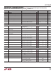
ELECTRICAL CHARACTERISTICS
The ● denotes specifications which apply over the full operating
temperature range, otherwise specifications are at T
A
= 25°C. V
CC
= 5V (Notes 2, 3)
SYMBOL PARAMETER CONDITIONS MIN TYP MAX UNITS
V.10 Receiver
V
TH
Receiver Input Threshold Voltage 0°C ≤ T
A
≤ 70°C ● –0.2 0.2 V
–7V ≤ V
CM
≤ 7V, –40°C ≤ T
A
≤ 85°C ● –0.3 0.3 V
∆V
TH
Receiver Input Hysteresis ● 11 50 mV
I
IN
Receiver Input Current –10V ≤ V
A
≤ 10V ● ±0.50 mA
R
IN
Receiver Input Impedance –10V ≤ V
A
≤ 10V ● 20 30 kΩ
t
r
, t
f
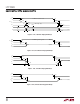
Rise or Fall Time (Figures 5, 9) 15 ns
t
PLH
Input to Output (Figures 5, 9) 350 ns
t
PHL
Input to Output (Figures 5, 9) 350 ns
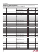
V.28 Driver
V
O
Output Voltage Open Circuit ±10 V
R
L
= 3k (Figure 4) ● ±5 7.6 V
I
SS
Short-Circuit Current V
O
= GND ● ±150 mA
I
OZ
Output Leakage Current –0.25V ≤ V
O
≤ 0.25V, Power Off or ● ±0.01 ±100 µA
No-Cable Mode or Driver Disabled
SR Slew Rate (Figures 4, 8), R
L
= 3k, C
L
= 2500pF ● 4.0 30.0 V/µs
t
PLH
Input to Output (Figures 4, 8), R
L
= 3k, C
L
= 2500pF ● 1.6 2.5 µs
t
PHL
Input to Output (Figures 4, 8), R
L
= 3k, C
L
= 2500pF ● 1.6 2.5 µs
V.28 Receiver
V
THL
Input Low Threshold Voltage ● 1.4 0.8 V
V
TLH
Input High Threshold Voltage ● 2.0 1.4 V
∆V
TH
Receiver Input Hysteresis ● 0.1 0.4 1.0 V
R
IN
Receiver Input Impedance –15V ≤ V
A
≤ 15V ● 357 kΩ
t
r
, t
f
Rise or Fall Time (Figures 5, 9) 15 ns
t
PLH
Input to Output (Figures 5, 9), CTRL = 0V 110 ns
CTRL = V
CC
● 330 800 ns
t
PHL
Input to Output (Figures 5, 9), CTRL = 0V 170 ns
CTRL = V
CC
● 480 800 ns