
Datasheet


12
LTC1344A
LINEAR TECHNOLOGY CORPORATION 1998
1344af, sn1344a LT/TP 0898 4K • PRINTED IN USA
Linear Technology Corporation
1630 McCarthy Blvd., Milpitas, CA 95035-7417
(408) 432-1900
●
FAX: (408) 434-0507
●
www.linear-tech.com
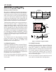
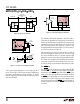
Figure 13 shows a typical application for the LTC1344A
using the LTC1543 mixed mode transceiver chip to gener-
ate the clock and data signals for a serial interface. The
LTC1344A V
EE
supply is generated from the LTC1543
charge pump and the select lines M0, M1, M2 and
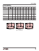
RELATED PARTS
PART NUMBER DESCRIPTION COMMENTS
LTC1334 Single Supply RS232/RS485 Transceiver 2 RS485 Dr/Rx or 4 RS232 Dr/Rx Pairs
LTC1343 Multiprotocol Serial Transceiver Software Selectable Mulitprotocol Interface
LTC1345 Single Supply V.35 Transceiver 3 Dr/3 Rx for Data and CLK Signals
LTC1346A Dual Supply V.35 Transceiver 3 Dr/3 Rx for Data and CLK Signals
LTC1543 Multiprotocol Serial Transceiver Software-Selectable Transceiver for Data and CLK Signals
LTC1544 Multiprotocol Serial Transceiver Software-Selectable Transceiver for Control Signals
DCE/DTE are shared by both chips. Each driver output and
receiver input is connected to one of the LTC1344A
termination ports. Each electrical protocol can then be
chosen using the digital select lines.
TYPICAL APPLICATIO
U
Figure 13. Typical Application Using the LTC1344A
LTC1543
24
1344 F13
426
5
6
7
8
9
10
23
22
21
20
19
18
17
16
15
M0
M1
M2
DCE/DTE
11
12
13
14
LTC1344A
14
21
22
23
24
1
2
5
3
8
11
12 13
4
6
7
9
10
16
15
18
17
19
20
DTE DCE
TXD
+
RXD
+
TXD
–
RXD
–
RXD
+
TXD
+
RXD
–
TXD
–
SCTE
+
RXC
+
SCTE
–
RXC
–
TXC
+
TXC
+
RXC
+
SCTE
+
RXC
–
SCTE
–
TXC
–
TXC
–
V
CC
V
EE
M2
M1
M0
C2
3.3µF
C1
1µF
100pF
100pF
100pF
LATCH
DCE/DTE
M2
M1
M0
DCE/DTE