
Datasheet


2
LTC1344A
ABSOLUTE MAXIMUM RATINGS
W
WW
U
WU
U
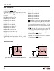
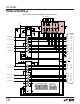
PACKAGE
/
O
RDER I FOR ATIO
ORDER PART
NUMBER
LTC1344ACG
LTC1344AIG
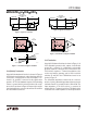
1
2
3
4
5
6
7
8
9
10
11
12
TOP VIEW
G PACKAGE
24-LEAD PLASTIC SSOP
24
23
22
21
20
19
18
17
16
15
14
13
M0
V
EE
R1C
R1B
R1A
R2A
R2B
R2C
R3A
R3B
R3C
GND
M1
M2
DCE/DTE
LATCH
R6B
R6A
R5A
R5B
R4A
R4B
V
CC
GND
T
JMAX
= 150°C, θ
JA
= 100°C/W
Consult factory for Military grade parts.
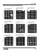
ELECTRICAL CHARACTERISTICS
V
CC
= 5V ±5%, V
EE
= –5V ±5%, T
A
= T
MIN
to T
MAX
(Notes 2, 3) unless otherwise noted.
(Note 1)
Positive Supply Voltage (V
CC
)................................... 7V
Negative Supply Voltage (V
EE
)........................... –13.2V
Input Voltage
(Logic Inputs).................... (V
EE
– 0.3V) to (V
CC
+ 0.3V)
Input Voltage (Load Inputs).................................. ±18V
Power Dissipation.............................................. 600mW
Operating Temperature Range
LTC1344AC ............................................ 0°C to 70°C
LTC1344AI ......................................... –40°C to 85°C
Storage Temperature Range................ –65°C to 150°C
Lead Temperature (Soldering, 10 sec)................. 300°C
Note 2: All currents into device pins are positive; all currents out of device
pins are negative. All voltages are reference to ground unless otherwise
specified.
Note 3: All typicals are given at V
CC
= 5V, V
EE
= –5V, T
A
= 25°C.
The ● denotes specifications which apply over the full operating
temperature range.
Note 1: Absolute Maximum Ratings are those values beyond which the life
of a device may be impaired.
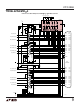
SYMBOL PARAMETER CONDITIONS MIN TYP MAX UNITS
Supplies
I
CC
Supply Current All Digital Pins = GND or V
CC
● 0.4 1.0 mA
Terminator Pins
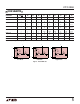
R
V.35
Differential Mode Impedance All Loads (Figure 1), –2V ≤ V
CM
≤ 2V (Commercial) ● 90 104 110 Ω
Common Mode Impedance All Loads (Figure 2), –2V ≤ V
CM
≤ 2V (Commercial) ● 135 153 165 Ω
All Loads (Figure 1), –2V ≤ V
CM
≤ 2V (Industrial) ● 90 104 115 Ω
All Loads (Figure 2), –2V ≤ V
CM
≤ 2V (Industrial) ● 130 153 170 Ω
R
V.11
Differential Mode Impedance All Loads (Figure 1), V
CM
= 0V (Commercial) ● 100 104 110 Ω
All Loads (Figure 1), –7V ≤ V
CM
≤ 7V (Commercial) 100 104 Ω
All Loads (Figure 1), V
CM
= 0V (Industrial) ● 95 104 115 Ω
All Loads (Figure 1), –7V ≤ V
CM
≤ 7V (Industrial) 100 104 Ω
I
LEAK
High Impedance Leakage Current All Loads, –7V ≤ V
CM
≤ 7V ● ±1 ±50 µA
Logic Inputs
V
IH
Input High Voltage All Logic Input Pins ● 2V
V
IL
Input Low Voltage All Logic Input Pins ● 0.8 V
I
IN
Input Current All Logic Input Pins ● ±10 µA