
Datasheet


4
LTC1344
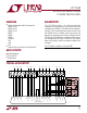
TEST CIRCUITS
PIN FUNCTIONS
UUU
M0 (Pin 1): TTL Level Mode Select Input. The data on M0
is latched when LATCH is high.
V
EE
(Pin 2): Negative Supply Voltage Input. Can connect
directly to the LTC1343 V
EE
pin.
R1C (Pin 3): Load 1 Center Tap.
R1B (Pin 4): Load 1 Node B.
R1A (Pin 5): Load 1 Node A.
R2A (Pin 6): Load 2 Node A.
R2B (Pin 7): Load 2 Node B.
R2C (Pin 8): Load 2 Center Tap.
R3A (Pin 9): Load 3 Node A.
R2B (Pin 10): Load 2 Node B.
R3C (Pin 11): Load 3 Center Tap.
GND (Pin 12): Ground Connection for Load 1 to Load 3.
GND (Pin 13): Ground Connection for Load 4 to Load 6.
V
CC
(Pin 14): Positive Supply Input. 4.75V ≤ V
CC
≤ 5.25V.
R4B (Pin 15): Load 4 Node B.
R4A (Pin 16): Load 4 Node A.
R5B (Pin 17): Load 5 Node B.
R5A (Pin 18): Load 5 Node A.
R6A (Pin 19): Load 6 Node A.
R6B (Pin 20): Load 6 Node B.
LATCH (Pin 21): TTL Level Logic Signal Latch Input. When
it is low the input buffers on M0, M1, M2 and DCE/DTE are
transparent. When it is high the logic pins are latched into
their respective input buffers. The data latch allows the
select lines to be shared between multiple I/O ports.
DCE/DTE (Pin 22): TTL Level Mode Select Input. The DCE
mode is selected when it is high and DTE mode when low.
The data on DCE/DTE is latched when LATCH is high.
M2 (Pin 23): TTL Level Mode Select Input 1. The data on
M2 is latched when LATCH is high.
M1 (Pin 24): TTL Level Mode Select Input 2. The data on
M1 is latched when LATCH is high.
R1
51.5Ω
R2
51.5Ω
±7V OR ±2V
1344 F01
R3
124Ω
S2
OFF
S1
ON
C
V
Ω
A
B
R1
51.5Ω
R2
51.5Ω
±2V
1344 F02
R3
124Ω
S2
ON
S1
ON
C
V
Ω
A, B
Figure 1. Differential V.11 or V.35 Impedance Measurement Figure 2. V.35 Common Mode Impedance Measurement