
Datasheet


9
LTC1344
TYPICAL APPLICATIONS N
U
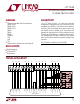
Figure 13 shows a typical application for the LTC1344
using the LTC1343 mixed mode transceiver chip to gener-
ate the clock and data signals for a serial interface. The
LTC1344 V
EE
supply is generated from the LTC1343
charge pump and the select lines M0, M1, M2, DCE and
LATCH are shared by both chips. Each driver output and
receiver input is connected to one of the LTC1344 termi-
nation ports. Each electrical protocol can then be chosen
using the digital select lines.
LTC1343
38
1344 F13
3842
6
7
9
13
14
15
37
36
35
34
33
32
31
30
29
28
27
M0
M1
M2
DCE/DTE
LATCH
17
18
19
21
22
LTC1344
14
21
22
23
24
1
2
5V
5
3
8
11
12 13
4
6
7
9
10
16
15
18 17 19 20
DTE DCE
TXD
+
RXD
+
TXD
–
RXD
–
RXD
+
TXD
+
RXD
–
TXD
–
SCTE
+
TXC
+
SCTE
–
TXC
–
NC RXC
+
NC RXC
–
RXC
+
NC
RXC
–
NC
TXC
+
SCTE
+
TXC
–
SCTE
–
V
CC
V
EE
M2
M1
M0
C2
3.3µF
C1
1µF
100pF
100pF
100pF
LATCH
DCE/DTE
M2
M1
M0
LATCH
DCE/DTE
+
Figure 13. Typical Application Using the LTC1344