
Datasheet


8
LTC1345
Theory of Operation
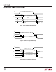
The transmitter output consists of complementary
switched-current sources as shown in Figure 7.
Figure 7. Simplified Transmitter Schematic
11mA
11mA
LTC1345 • F07
Y
Z
T
50Ω
125Ω
50Ω
V
CC
V
EE
CHIP
BOUNDARY
With a logic zero at the transmitter input, the inverting
output Z sources 11mA and the noninverting output Y
sinks 11mA. The differential transmitter output voltage is
then set by the termination resistors. With two differential
50Ω resistors at each end of the cable, the voltage is set to
(50Ω × 11mA) = 0.55V. With a logic 1 at the transmitter
input, output Z sinks 11mA and Y sources 11mA. The
common-mode voltage of Y and Z is 0V when both current
sources are matched and there is no ground potential
difference between the cable terminations. The transmitter
current sources have a common-mode range of ±2V,
which allows for a ground difference between cable termi-
nations of ±4V.
Each receiver input has a 30k resistance to ground and
requires external termination to meet the V.35 input imped-
ance specification. The receivers have an input hysteresis
of 50mV to improve noise immunity. The receiver output
may be forced into a high impedance state by pulling the
output enable (OE) pin high. For normal operation OE
should be pulled low.
A charge pump generates the regulated negative supply
voltage (V
EE
) with three 1µF capacitors. Commutating
capacitors C1 and C2 form a voltage doubler and inverter
while C3 acts as a reservoir capacitor. To insure proper
operation, the capacitors must have an ESR less than 1Ω.
Monolithic ceramic or solid tantalum capacitors are good
choices. Under light loads, regulation at about –5.2V is
provided by a pulse-skipping scheme. Under heavy loads
the charge pump is on continuously. A small ripple of about
500mV will be present on V
EE
.
Two Select pins, S1 and S2, configure the chip for DTE,
DCE, all transmitters and receivers on, or Shutdown. In
Shutdown mode, I
CC
drops to 1µA. The outputs of the
transmitters and receivers are in high impedance states,
the charge pump stops and V
EE
is clamped to ground.
ESD Protection
LTC1345 transmitter outputs and receiver inputs have on-
chip protection from multiple ±10kV ESD transients. ESD
testing is done using the Human Body ESD Model. ESD
testing must be done with an AC ground on the V
CC
and V
EE
supply pins. The low ESR supply decoupling and V
EE
reservoir capacitors provide this AC ground during normal
operation.
Complete V.35 Port
Figure 8 shows the schematic of a complete surface
mounted, single 5V DTE and DCE V.35 port using only
three ICs and eight capacitors per port. The LTC1345 is
used to transmit the clock and data signals, and the
LT1134A to transmit the control signals. If test signals
140, 141, and 142 are not used, the transmitter inputs
should be tied to V
CC
.
APPLICATIO S I FOR ATIO
WUUU