
Datasheet


4
LTC1383
1383fa
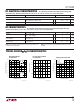
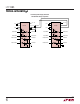
TYPICAL PERFOR A CE CHARACTERISTICS
UW
V
CC
Supply Current
vs Temperature
TEMPERATURE (°C)
0
0
SUPPLY CURRENT (mA)
2
6
8
10
40
18
LTC1383 • TPC04
4
20
10
50
30 60 70
12
14
16
2 DRIVERS LOADED
R
L
= 3k
1 DRIVER LOADED
R
L
= 3k
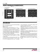
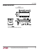
Driver Output Waveforms Receiver Output Waveforms
INPUT
LTC1383 • TPC05
RECEIVER
OUTPUT
C
L
= 51pF
INPUT
LTC1383 • TPC06
V
CC
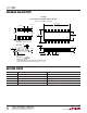
: 5V Input Supply Pin. This pin should be decoupled
with a 0.1µF ceramic capacitor.
GND: Ground Pin.
V
+
: Positive Supply Output (RS232 Drivers). V
+
≅ 2V
CC
–
2V. This pin requires an external capacitor C = 0.1µF for
charge storage. The capacitor may be tied to ground or
V
CC
. With multiple devices, the V
+
and V
–
pins may share
a common capacitor. For large numbers of devices, in-
creasing the size of the shared common storage capaci-
tors is recommended to reduce ripple.
V
–
: Negative Supply Output (RS232 Drivers). V
–
≅ – (2V
CC
– 2V). This pin requires an external capacitor C = 0.1µF for
charge storage.
C1
+
, C1
–
, C2
+
, C2
–
: Commutating Capacitor Inputs. These
pins require two external capacitors C = 0.1µF: one from
C1
+
to C1
–
and another from C2
+
to C2
–
. To maintain
charge pump efficiency, the capacitor’s effective series
resistance should be less than 2Ω.
TR IN: RS232 Driver Input Pins. Inputs are TTL/CMOS
compatible. The inputs of unused drivers can be left
unconnected since 300k input pull-up resistors to V
CC
are
included on chip.
TR OUT: Driver Outputs at RS232 Voltage Levels. The
driver outputs are protected against ESD to ±10kV for
human body model discharges.
RX IN: Receiver Inputs. These pins can be forced to ±25V
without damage. The receiver inputs are protected against
ESD to ±10kV for human body model discharges. Each
receiver provides 0.4V of hysteresis for noise immunity.
RX OUT: Receiver Outputs with TTL/CMOS Voltage
Levels.
DRIVER
OUTPUT
R
L
= 3k
C
L
= 2500pF
DRIVER
OUTPUT
R
L
= 3k
5µs/DIV 5µs/DIV
UU
U
PI FU CTIO S