
Datasheet


4
LTC1386
1386fa
V
CC
: 3.3V Input Supply Pin. This pin should be decoupled
with a 0.1µF ceramic capacitor.
GND: Ground Pin.
V
+
: Positive Supply Output (EIA/TIA562 Drivers). V
+
≅
2V
CC
– 1V. This pin requires an external capacitor C =
0.1µF for charge storage. The capacitor may be tied to
ground or V
CC
. With multiple devices, the V
+
and V
–
pins
may share a common capacitor. For large numbers of
devices, increasing the size of the shared common storage
capacitors is recommended to reduce ripple.
V
–
: Negative Supply Output (RS232 Drivers). V
–
≅ – (2V
CC
– 1.3V). This pin requires an external capacitor C = 0.1µF
for charge storage.
C1
+
, C1
–
, C2
+
, C2
–
: Commutating Capacitor Inputs. These
pins require two external capacitors C = 0.1µF: one from
C1
+
to C1
–
and another from C2
+
to C2
–
. To maintain
charge pump efficiency, the capacitor’s effective series
resistance should be less than 2Ω.
TR IN: EIA/TIA562 Driver Input Pins. Inputs are TTL/
CMOS compatible. The inputs of unused drivers can be left
unconnected since 300k input pull-up resistors to V
CC
are
included on chip.
TR OUT: Driver Outputs at EIA/TIA562 Voltage Levels.
The driver outputs are protected against ESD to ±10kV for
human body model discharges.
RX IN: Receiver Inputs. These pins can be forced to ±25V
without damage. The receiver inputs are protected against
ESD to ±10kV for human body model discharges. Each
receiver provides 0.4V of hysteresis for noise immunity.
RX OUT: Receiver Outputs with TTL/CMOS Voltage
Levels.
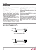
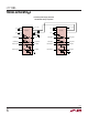
Figure 1. Driver Propagation Delay Timing
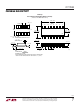
Figure 2. Receiver Propagation Delay Timing
SWITCHI G TI E WAVEFOR S
UWW
1.4V
0V
V
CC
0V
V
+
V
–
0V
DRIVER
INPUT
DRIVER
OUTPUT
1.4V
t
HLD
t
LHD
LTC1386 • F01
0.8V
V
CC
0V
2.4V
RX
INPUT
RX
OUTPUT
1.3V
t
HLR
1.7V
t
LHR
LTC1386 • F02
V
CC
0V
UU
U
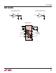
PI FU CTIO S