
Datasheet

1
LTC1391
sn1391 1391fas
8-Channel
Analog Multiplexer with
Cascadable Serial Interface
■
Low R
ON
: 45Ω
■
Single 2.7V to ±5V Supply Operation
■
Low Charge Injection
■
Serial Digital Interface
■
Analog Inputs May Extend to Supply Rails
■
Low Leakage: ±5nA Max
■
Guaranteed Break-Before-Make
■
TTL/CMOS Compatible for All Digital Inputs
■
Cascadable to Allow Additional Channels
■
Can Be Used as a Demultiplexer
The LTC
®
1391 is a high performance CMOS 8-to-1 analog
multiplexer. It features a serial digital interface that allows
several LTC1391s to be daisy-chained together, increas-
ing the number of MUX channels available using a single
digital port.
The LTC1391 features a typical R
ON
of 45Ω, a typical
switch leakage of 50pA and guaranteed break-before-
make operation. Charge injection is ±10pC maximum. All
digital inputs are TTL and CMOS compatible when oper-
ated from single or dual supplies. The inputs can with-
stand 100mA fault current.
The LTC1391 is available in 16-pin PDIP, SSOP and
narrow SO packages. For applications requiring 2-way
serial data transmission, see the LTC1390 data sheet.
■
Data Acquisition Systems
■
Communication Systems
■
Signal Multiplexing/Demultiplexing
, LTC and LT are registered trademarks of Linear Technology Corporation.
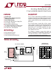
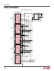
1
2
3
4
5
6
7
8
16
15
14
13
12
11
10
9
S0
S1
S2
S3
S4
S5
S6
S7
V
+
D
V
–
D
OUT
D
IN
CS
CLK
GND
ANALOG
INPUTS
LTC1391
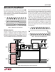
1
2
3
4
8
7
6
5
V
CC
CLK
D
OUT
CS/SHDN
V
REF
+IN
–IN
GND
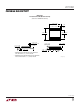
LTC1285
3V
0.1µF
OPTIONAL A/D
INPUT FILTER
1µF
DATA IN
CLK
CS
DATA OUT
SERIAL INTERFACE
TO MUX AND ADC
1391 TA01
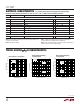
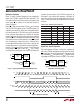
ANALOG INPUT VOLTAGE (V)
–5 –4 –2 0 2 4
ON-RESISTANCE (Ω)
300
250
200
150
100
50
0
–3 –1 1 3
1391 TA02
5
T
A
= 25°C
V
+
= 2.7V
V
–
= 0V
V
+
= 5V
V
–
= –5V
On-Resistance vs
Analog Input Voltage
3V, 8-Channel 12-Bit ADC
FEATURES
DESCRIPTIO
U
APPLICATIO S
U
TYPICAL APPLICATIO
U