
Datasheet

4
LTC1391
sn1391 1391fas
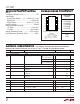
ELECTRICAL CHARACTERISTICS
The ● denotes the specifications which apply over the full operating
temperature range, otherwise specifications are at T
A
= 25°C. V
+
= 2.7V, V
–
= GND = 0V, unless otherwise specified.
Note 1: Absolute Maximum Ratings are those values beyond which the life
of a device may be impaired.
Note 2: Guaranteed by Design.
Note 3: Leakage current with a single 2.7V supply is guaranteed by
correlation with the ±5V leakage current specifications.
Note 4: Timing specifications with a single 2.7V supply are guaranteed by
correlation with the ±5V timing specifications.
SYMBOL PARAMETER CONDITIONS MIN TYP MAX UNITS
Dynamic
f
CLK
Clock Frequency (Note 2) 5 MHz
t
ON
Enable Turn-On Time V
S
= 1.5V, R
L
= 1k, C
L
= 35pF (Note 4) 490 800 ns
t
OFF
Enable Turn-Off Time V
S
= 1.5V, R
L
= 1k, C
L
= 35pF (Note 4) 190 400 ns
t
OPEN
Break-Before-Make Interval (Note 4) 125 290 ns
QIRR Off Isolation V
S
= 2V
P–P
, R
L
= 1k, f = 100kHz 70 dB
Q
INJ
Charge Injection R
S
= 0, C
L
= 1000pF, V
S
= 1V (Note 2) ±1 ±5pC
C
S(OFF)
Input Off Capacitance 5pF
C
D(OFF)
Output Off Capacitance 10 pF
Supply
I
+
Positive Supply Current All Logic Inputs Tied Together, V
IN
= 0V or 2.7V ● 0.2 2 µA
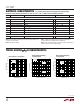
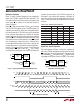
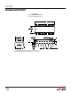
TEMPERATURE (°C)
–40 –20
ON-RESISTANCE (Ω)
300
250
200
150
100
50
0
80
1391 G01
0
20 40 60
V
+
= 2.7V
V
–
= 0V
V
S
= 1.2V
V
+
= 5V
V
–
= –5V
V
S
= 0V
On-Resistance vs Temperature
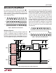
TEMPERATURE (°C)
–40
OUTPUT VOLTAGE (V)
0.65
0.60
0.55
0.50
0.45
0.40
0.35
0.30
0.25
0.20
0.15
0.10
60
1391 G03
–20
020
40
80
V
+
= 5V
V
–
= –5V
I
O
= 1.8mA
V
+
= 2.7V
V
–
= 0V
I
O
= 400µA
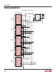
OUTPUT CURRENT (mA)
0
OUTPUT VOLTAGE (V)
0.4
0.8
1.0 2.01.8
1391 G02
0.2 0.6
1.2
1.4
1.6
1.2
1.1
1.0
0.9
0.8
0.7
0.6
0.5
0.4
0.3
0.2
0.1
0
T
A
= 25°C
V
+
= 2.7V
V
–
= 0V
V
+
= 5V
V
–
= –5V
Driver Output Low Voltage
vs Output Current
Driver Output Low Voltage
vs Temperature
TYPICAL PERFOR A CE CHARACTERISTICS
UW