
Datasheet

5
LTC1391
sn1391 1391fas
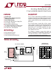
PIN FUNCTIONS
UUU
S0, S1, S2, S3, S4, S5, S6, S7 (Pins 1, 2, 3, 4, 5, 6, 7,
8): Analog Multiplexer Inputs.
GND (Pin 9): Digital Ground. Connect to system ground.
CLK (Pin 10): System Clock (TTL/CMOS Compatible). The
clock synchronizes the channel selection bits and the
serial data transfer from D
IN
to D
OUT
.
CS (Pin 11): Channel Select Input (TTL/CMOS Compat-
ible). A logic high on this input enables the LTC1391 to
read in the channel selection bits and allows digital data
transfer from D
IN
to D
OUT
. A logic low on this input puts
D
OUT
into three-state and enables the selected channel for
analog signal transmission.
D
IN
(Pin 12): Digital Input (TTL/CMOS Compatible). Input
for the channel selection bits.
D
OUT
(Pin 13): Digital Output (TTL/CMOS Compatible).
Output from the internal shift register.
V
–
(Pin 14): Negative Supply. For ±5V dual supply appli-
cations, |V
–
| should not exceed |V
+
|by more than 20% for
proper channel selection.
D (Pin 15): Analog Multiplexer Output.
V
+
(Pin 16): Positive Supply.
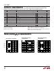
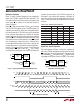
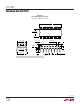
TYPICAL PERFOR A CE CHARACTERISTICS
UW
OUTPUT VOLTAGE (V)
2.0 2.5
OUTPUT CURRENT (mA)
3.0 4.03.5
4.5
5.0
1391 G04
0
–0.5
–1.0
–1.5
–2.0
–2.5
–3.0
–3.5
–4.0
V
+
= 5V
V
–
= –5V
T
A
=25°C
V
+
= 2.7V
V
–
= 0V
TEMPERATURE (°C)
–40
OUTPUT VOLTAGE (V)
5.0
4.5
4.0
3.5
3.0
2.5
2.0
1.5
1.0
0.5
0
60
1391 G05
–20
020
40
80
V
+
= 5V
V
–
= –5V
I
O
= 1.6mA
V
+
= 2.7V
V
–
= 0V
I
O
= 400µA
Driver Output High Voltage
vs Output Current
Driver Output High Voltage
vs Temperature