
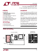
Datasheet

6
LTC1391
sn1391 1391fas
APPLICATIONS INFORMATION
WUU
U
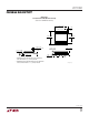
Multiplexer Operation
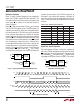
Figure 1 shows the block diagram of the components
within the LTC1391 required for MUX operation. The
LTC1391 uses D
IN
to select the active channel and the chip
select input, CS, to switch on the selected channel as
shown in Figure 2.
When CS is high, the input data on the D
IN
pin is latched
into the 4-bit shift register on the rising clock edge. The
input data consists of the “EN” bit and a string of three bits
for channel selection. If “EN” bit is logic high as illustrated
in the first input data sequence, it enables the selected
channel. After the clocking in of the last channel selection
bit B0, the CS pin must be pulled low before the next rising
clock edge to ensure correct operation. Once CS is pulled
low, the previously selected channel is switched off to
ensure a break-before-make interval. After a delay of t
ON
,
the selected channel is switched on allowing signal trans-
mission. The selected channel remains on until the next
falling edge of CS. After a delay of t
OFF
, the LTC1391
terminates the analog signal transmission and allows the
selection of next channel. If the “EN” bit is logic low, as
illustrated in the second data sequence, it disables all
channels and there will be no analog signal transmission.
Table 1 shows the various bit combinations for channel
selection.
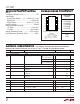
Table 1. Logic Table for Channel Selection
ACTIVE CHANNEL EN B2 B1 BO
All Off 0 X X X
S0 1 0 0 0
S1 1 0 0 1
S2 1 0 1 0
S3 1 0 1 1
S4 1 1 0 0
S5 1 1 0 1
S6 1 1 1 0
S7 1 1 1 1
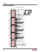
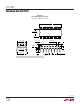
Digital Data Transfer Operation
The block diagram of Figure 3 shows the components
within the LTC1391 required for serial data transfer. When
CS is held high, data is fed into the 4-bit shift register and
then shifted to D
OUT
. Data appears at D
OUT
after the fourth
rising edge of the clock as shown in Figure 4. The last four
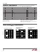
Figure 2. Multiplexer Operation
EN
HIGH
B2
EN LO
B2 B1 B0B1 B0
CLK
CS
D
IN
ANY ANALOG
INPUT
D
t
ON
t
OFF
1391 • F02
Figure 1. Simplified Block Diagram of the MUX Operation
CONTROL
LOGIC
4-BIT SHIFT
REGISTER
MUX
BLOCK
CLK
D
IN
CS
1391 • F01
ANALOG
OUTPUT (D)
ANALOG INPUTS
(S0 TO S7)
Figure 3. Simplified Block Diagram of the
Digital Data Transfer Operation
CONTROL
LOGIC
4-BIT SHIFT
REGISTER
CLK
D
IN
CS
1391 F03
D
OUT