
Datasheet

LTC1403-1/LTC1403A-1
14
14031fc
APPLICATIONS INFORMATION
Board Layout and Bypassing
Wire wrap boards are not recommended for high resolu-
tion and/or high speed A/D converters. To obtain the best
performance from the LTC1403-1/LTC1403A-1, a printed
circuit board with ground plane is required. Layout for
the printed circuit board should ensure that digital and
analog signal lines are separated as much as possible.
In particular, care should be taken not to run any digital
track alongside an analog signal track. If optimum phase
match between the inputs is desired, the length of the two
input wires should be kept matched.
High quality tantalum and ceramic bypass capacitors
should be used at the V
DD
and V
REF
pins as shown in the
Block Diagram on the first page of this data sheet. For op-
timum performance, a 10µF surface mount AVX capacitor
with a 0.1µF ceramic is recommended for the V
DD
and V
REF
pins. Alternatively, 10µF ceramic chip capacitors such as
Murata GRM219R60J106M may be used. The capacitors
must be located as close to the pins as possible. The traces
connecting the pins and the bypass capacitors must be
kept short and should be made as wide as possible.
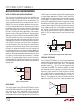
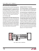
Figure 7 shows the recommended system ground connec-
tions. All analog circuitry grounds should be terminated at
the LTC1403-1/LTC1403A-1 GND (Pins 4, 5, 6 and exposed
pad). The ground return from the LTC1403-1/LTC1403A-1
(Pins 4, 5, 6 and exposed pad) to the power supply
should be low impedance for noise free operation. Digital
circuitry grounds must be connected to the digital supply
common. In applications where the ADC data outputs and
control signals are connected to a continuously active
microprocessor bus, it is possible to get errors in the
conversion results. These errors are due to feedthrough
from the microprocessor to the successive approximation
comparator. The problem can be eliminated by forcing the
microprocessor into a Wait state during conversion or by
using three-state buffers to isolate the ADC data bus.
POWER-DOWN MODES
Upon power-up, the LTC1403-1/LTC1403A-1 is initialized
to the active state and is ready for conversion. The Nap
and Sleep mode waveforms show the power-down modes
for the LTC1403-1/LTC1403A-1. The SCK and CONV inputs
control the power-down modes (see Timing Diagrams).
Two rising edges at CONV, without any intervening ris-
ing edges at SCK, put the LTC1403-1/LTC1403A-1 in Nap
mode and the power drain drops from 14mW to 6mW.
The internal reference remains powered in Nap mode.
Figure 7. Recommended Layout
14031 F07
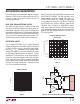
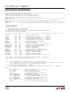
FREQUENCY (Hz)
MAGNITUDE (dB)
–60
–30
–20
14031 F06b
–70
–80
–120
–100
0
–10
–40
–50
–90
–110
0
371k185k 556k 741k
Figure 6b. LTC1403-1 6MHz Sine Wave 4096 Point FFT Plot
with the LT1819 Driving the Inputs Differentially