
Datasheet
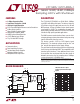


LTC1403-1/LTC1403A-1
5
14031fc
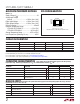
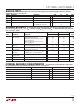
ELECTRICAL CHARACTERISTICS
Note 1: Stresses beyond those listed under Absolute Maximum Ratings
may cause permanent damage to the device. Exposure to any Absolute
Maximum Rating condition for extended periods may affect device
reliability and lifetime.
Note 2: All voltage values are with respect to GND.
Note 3: When these pins are taken below GND or above V
DD
, they will be
clamped by internal diodes. This product can handle input currents greater
than 100mA below GND or greater than V
DD
without latchup.
Note 4: Offset and full-scale specifications are measured for a single-
ended A
IN
+
input with A
IN
–
grounded and using the internal 2.5V reference.
Note 5: Integral linearity is tested with an external 2.55V reference and is
defined as the deviation of a code from the straight line passing through
the actual endpoints of a transfer curve. The deviation is measured from
the center of quantization band.
Note 6: Guaranteed by design, not subject to test.
Note 7: Recommended operating conditions.
Note 8: The analog input range is defined for the voltage difference
between A
IN
+
and A
IN
–
. Performance is specified with A
IN
–
= 1.5V DC while
driving A
IN
+
.
Note 9: The absolute voltage at A
IN
+
and A
IN
–
must be within this range.
Note 10: If less than 3ns is allowed, the output data will appear one
clock cycle later. It is best for CONV to rise half a clock before SCK, when
running the clock at rated speed.
Note 11: Not the same as aperture delay. Aperture delay is smaller (1ns)
because the 2.2ns delay through the sample-and-hold is subtracted from
the CONV to Hold mode delay.
Note 12: The rising edge of SCK is guaranteed to catch the data coming
out into a storage latch.
Note 13: The time period for acquiring the input signal is started by the
16th rising clock and it is ended by the rising edge of convert.
Note 14: The internal reference settles in 2ms after it wakes up from Sleep
mode with one or more cycles at SCK and a 10µF capacitive load.
Note 15: The full power bandwidth is the frequency where the output code
swing drops to 3dB with a 2.5V
P-P
input sine wave.
Note 16: Maximum clock period guarantees analog performance during
conversion. Output data can be read without an arbitrarily long clock.
Note 17: V
DD
= 3V, f
SAMPLE
= 2.8Msps.
Note 18: The LTC1403A-1 is measured and specified with 14-bit
Resolution (1LSB = 152µV) and the LTC1403-1 is measured and specified
with 12-bit Resolution (1LSB = 610µV).
Note 19: Full-scale sinewaves are fed into the noninverting input while the
inverting input is kept at 1.5V DC.
Note 20: The sampling capacitor at each input accounts for 4.1pF of the
input capacitance.