
Datasheet


2
LTC1408
1408fa
A
U
G
W
A
W
U
W
ARB
S
O
LU
T
EXI T
I
S
(Notes 1, 2)
Supply Voltage (V
DD
, V
CC
, OV
DD
) .............................. 4V
Analog Input Voltage
(Note 3) ................................... – 0.3V to (V
DD
+ 0.3V)
Digital Input Voltage .................... – 0.3V to (V
DD
+ 0.3V)
Digital Output Voltage .................. – 0.3V to (V
DD
+ 0.3V)
Power Dissipation.............................................. 100mW
Operation Temperature Range
LTC1408C ............................................... 0°C to 70°C
LTC1408I............................................ –40°C to 85°C
Storage Temperature Range ................. –65°C to 125°C
The ● denotes the specifications which apply over the full operating
temperature range, otherwise specifications are at T
A
= 25°C. With internal reference, V
DD
= 3V, V
DD
= V
CC
= 3V.
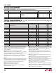
PARAMETER CONDITIONS MIN TYP MAX UNITS
Resolution (No Missing Codes) ● 14 Bits
Integral Linearity Error (Note 5) ● –3 ±0.5 3 LSB
Offset Error (Note 4) ● –4.5 ±1 4.5 mV
Offset Match from CH0 to CH5 –3 ±0.5 3 mV
Range Error (Note 4) ● –12 ±212 mV
Range Match from CH0 to CH5 –5 ±15 mV
Range Tempco Internal Reference (Note 4) ±15 ppm/°C
External Reference ±1 ppm/°C
The ● denotes the specifications which apply over the full operating temperature range,
otherwise specifications are at T
A
= 25°C. With internal reference, V
DD
= 3V, V
DD
= V
CC
= 3V.
SYMBOL PARAMETER CONDITIONS MIN TYP MAX UNITS
V
IN
Analog Differential Input Range (Notes 3, 8, 9) 2.7V ≤ V
DD
≤ 3.3V 0 to 2.5 V
V
CM
Analog Common Mode + Differential 0 to V
DD
V
Input Range (Note 8)
I
IN
Analog Input Leakage Current ● 1 µA
C
IN
Analog Input Capacitance 13 pF
t
ACQ
Sample-and-Hold Acquisition Time (Note 6) ● 39 ns
t
AP
Sample-and-Hold Aperture Delay Time 1 ns
t
JITTER
Sample-and-Hold Aperture Delay Time Jitter 0.3 ps
t
SK
Channel to Channel Aperture Skew 200 ps
CMRR Analog Input Common Mode Rejection Ratio f
IN
= 100kHz, V
IN
= 0V to 3V –83 dB
f
IN
= 10MHz, V
IN
= 0V to 3V –67 dB
CO VERTER CHARACTERISTICS
U
A ALOG I PUT
UU
WU
U
PACKAGE
/
O
RDER I FOR ATIO
ORDER PART
NUMBER
QFN PART MARKING
T
JMAX
= 125°C, θ
JA
= 34°C/ W
EXPOSED PIN IS GND (PAD 33)
MUST BE SOLDERED TO PCB
Consult LTC Marketing for parts specified with wider operating temperature ranges.
16 15 14 13 12 11 10 9
25 26 27 28
TOP VIEW
QFN PACKAGE
32-PIN (5mm × 5mm) PLASTIC QFN
29 30 31 32
1
2
3
4
5
6
7
8
24
23
22
21
20
19
18
17CH4
+
CH4
–
GND
CH5
+
CH5
–
GND
V
REF
V
CC
CH1
–
CH1
+
GND
CH0
–
CH0
+
OV
DD
OGND
SDO
GND
CH3
–
CH3
+
GND
GND
CH2
–
CH2
+
GND
V
DD
SEL2
SEL1
SEL0
BIP
CONV
DGND
SCK
33
LTC1408CUH
LTC1408IUH
1408
Order Options Tape and Reel: Add #TR
Lead Free: Add #PBF Lead Free Tape and Reel: Add #TRPBF
Lead Free Part Marking: http://www.linear.com/leadfree/