
Datasheet


13
LTC1417
sn1417 1417fas
APPLICATIONS INFORMATION
WUU
U
capacitor from +A
IN
to ground and a 100Ω source resistor
to limit the input bandwidth to 1.6MHz. The 1000pF
capacitor also acts as a charge reservoir for the input
sample-and-hold and isolates the ADC input from sam-
pling glitch sensitive circuitry. High quality capacitors and
resistors should be used since these components can add
distortion. NPO and silver mica type dielectric capacitors
have excellent linearity. Carbon surface mount resistors can
also generate distortion from self heating and from damage
that may occur during soldering. Metal film surface mount
resistors are much less susceptible to both problems.
Input Range
The ±2.048V and 0V to 4.096V input ranges of the
LTC1417 are optimized for low noise and low distortion.
Most op amps also perform well over these ranges,
allowing direct coupling to the analog inputs and eliminat-
ing the need for special translation circuitry.
Some applications may require other input ranges. The
LTC1417 differential inputs and reference circuitry can
accommodate other input ranges often with little or no
additional circuitry. The following sections describe the
reference and input circuitry and how they affect the input
range.
INTERNAL REFERENCE
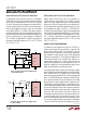
The LTC1417 has an on-chip, temperature compensated,
curvature corrected, bandgap reference which is factory
trimmed to 2.500V. It is internally connected to a reference
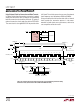
amplifier and is available at Pin 3. An 8k resistor is in series
with the output so that it can be easily overdriven in
applications where an external reference is required, see
Figure 9. A capacitor must be connected between the
reference amplifier compensation pin (REFCOMP, Pin 4)
and ground. The reference is stable with capacitors of 1µF
or greater. For the best noise performance, a 10µF in
parallel with a 0.1µF ceramic is recommended.
The V
REF
pin can be driven with a DAC or other means
to provide input span adjustment. The reference should
be kept in the range of 2.25V to 2.75V for specified linearity.
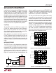
UNIPOLAR /BIPOLAR OPERATION AND ADJUSTMENT
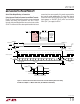
Figure 10a shows the input/output characteristics for the
LTC1417. The code transitions occur midway between
successive integer LSB values (i.e., 0.5LSB, 1.5LSB,
2.5LSB, … FS – 1.5LSB). The output code is natural binary
with 1LSB = FS/16384 = 4.096V/16384 = 250µV. Figure
10b shows the input/output transfer characteristics for the
bipolar mode in two’s complement format.
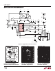
Figure 9. Using the LT1460 as an External Reference
ANALOG
INPUT
5V
1417 F09
10µF
2.5V
0.1µF
V
IN
V
OUT
LT1460-2.5
1
2
3
4
5
LTC1417
5V
A
IN
+
A
IN
–
V
REF
REFCOMP
AGND
V
DD
Figure 10a. LTC1417 Unipolar Transfer Characteristics
Figure 10b. LTC1417 Bipolar Transfer Characteristics
INPUT VOLTAGE (V)
0V
OUTPUT CODE
FS – 1LSB
1417 F10a
111...111
111...110
111...101
111...100
000...000
000...001
000...010
000...011
1
LSB
UNIPOLAR
ZERO
1LSB =
FS
16384
4.096V
16384
=
INPUT VOLTAGE (V)
0V
OUTPUT CODE
–1
LSB
1417 F10b
011...111
011...110
000...001
000...000
100...000
100...001
111...110
1
LSB
BIPOLAR
ZERO
111...111
FS/2 – 1LSB–FS/2
FS = 4.096V
1LSB = FS/16384