
Datasheet

21
LTC1417
sn1417 1417fas
1211109876543210
FILL
ZEROS
D13
t
2
t
3
12345678910111213141516
Hi-Z
DATA N
Hi-Z
(SAMPLE N)
D
OUT
EXTCLKIN = 5
CONVST
t
10
t
CONV
t
5
HOLD
SAMPLE
t
6
t
7
t
9
1417 F19
t
8
BUSY
SCLK
RD
D11D12
CAPTURE ON
RISING CLOCK
D13
t
12
t
11
t
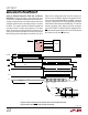
LSCLK
t
HSCLK
SCLK
V
IL
V
OH
V
OL
D
OUT
CAPTURE ON
FALLING CLOCK
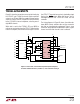
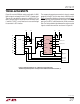
LTC1417
BUSYCONVST
1413
9
12
7
CONVST
RD
SCLK
D
OUT
µP OR DSP
INT
C0
SCK
MISO
APPLICATIONS INFORMATION
WUU
U
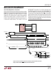
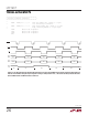
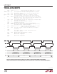
Figure 19. Internal Conversion Clock Selected. Data Transferred After Conversion
Using an External SCLK. BUSY↑ Indicates End of Conversion
MICROWIRE is a trademark of National Semiconductor Corporation.
Serial Data Output After a Conversion
Using an Internal Conversion Clock and an External Data
Clock. In this mode, data is output after the end of each
conversion and before the next conversion is started
(Figure 19). The internal clock is used as the conversion
clock and an external clock is used for the SCLK. This
mode is useful in applications where the processor acts as
a serial bus master device. This mode is SPI and
MICROWIRE
TM
compatible. It also allows operation when
the SCLK frequency is very low (less than 30kHz). To
select the internal conversion clock, tie EXTCLKIN high.
The external SCLK is applied to SCLK. RD can be used to
gate the external SCLK, such that data will clock only after
RD goes low and to three-state D
OUT
after data transfer. If
more than 16 SCLKs are provided, more zeros will be filled
in after the data word indefinitely.