
Datasheet

28
LTC1417
sn1417 1417fas
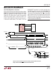
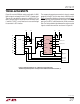
TYPICAL APPLICATIONS
U
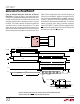
Listing B
*************************************************************************
* *
* This example program selects a DG408 MUX channel using parallel *
* port C, initiates a conversion, and retrieves data from the LTC1417. *
* It stores the 14-bit, right justified data in two consecutive memory *
* locations. *
* *
*************************************************************************
*
*****************************************
* 68HC11 register definitions *
*****************************************
*
PIOC EQU $1002 Parallel I/O control register
* “STAF,STAI,CWOM,HNDS, OIN, PLS, EGA,INVB”
PORTC EQU $1003 Port C data register
* “Bit7,Bit6,Bit5,Bit4,Bit3,Bit2,Bit1,Bit0”
DDRC EQU $1007 Port D data direction register
* “Bit7,Bit6,Bit5,Bit4,Bit3,Bit2,Bit1,Bit0”
* 1 = output, 0 = input
PORTD EQU $1008 Port D data register
* “ - , - , SS* ,CSK ;MOSI,MISO,TxD ,RxD “
DDRD EQU $1009 Port D data direction register
SPCR EQU $1028 SPI control register
* “SPIE,SPE ,DWOM,MSTR;SPOL,CPHA,SPR1,SPR0”
SPSR EQU $1029 SPI status register
* “SPIF,WCOL, - ,MODF; - , - , - , - “
SPDR EQU $102A SPI data register; Read-Buffer; Write-Shifter
*
* RAM variables to hold the LTC1417’s 14 conversion result
*
DIN1 EQU $00 This memory location holds the LTC1417’s bits 13 - 08
DIN2 EQU $01 This memory location holds the LTC1417’s bits 07 - 00
MUX EQU $02 This memory location holds the MUX address data
*
*****************************************
* Start GETDATA Routine *
*****************************************
*
ORG $C000 Program start location
INIT1 LDAA #$03 0,0,0,0,0,0,1,1
* “STAF=0,STAI=0,CWOM=0,HNDS=0, OIN=0, PLS=0, EGA=1,INVB=1”
STAA PIOC Ensures that the PIOC register’s status is the same
* as after a reset, necessary of simple Port D manipulation
LDAA #$47 0,1,0,0,0,1,1,1
* “Bit7=input,Bit6=output,- ,- ,- ,Bit2=output,Bit1=output,
* Bit0=output”
* Bit7 used for BUSY input
* Bit6 used for CONVST signal output
* Bits 2 - 0 are used for the MUX address
STAA DDRC Direction of PortD’s bit are now set
LDAA #$2F -,-,1,0;1,1,1,1
* -, -, SS*-Hi, SCK-Lo, MOSI-Hi, MISO-Hi, X, X
STAA PORTD Keeps SS* a logic high when DDRD, Bit5 is set
LDAA #$38 -,-,1,1;1,0,0,0
STAA DDRD SS* , SCK, MOSI are configured as Outputs
* MISO, TxD, RxD are configured as Inputs
* DDRD’s Bit5 is a 1 so that port D’s SS* pin is a general output
LDAA #$50
STAA SPCR The SPI is configured as Master, CPHA = 0, CPOL = 0
* and the clock rate is E/2
* (This assumes an E-Clock frequency of 4MHz. For higher