
Datasheet

13
LTC1435A
APPLICATIONS INFORMATION
WUU
U
on and off again. It is determined by internal timing delays
and the gate charge required to turn on the top MOSFET.
Low duty cycle applications may approach this minimum
on-time limit. If the duty cycle falls below what can be
accommodated by the minimum on-time, the LTC1435A
will begin to skip cycles. The output voltage will continue
to be regulated, but the ripple current and ripple voltage will
increase. Therefore this limit should be avoided.
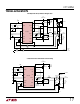
The minimum on-time for the LTC1435A in a properly
configured application is less than 300ns but increases at
low ripple current amplitudes (see Figure 7). If an appli-
cation is expected to operate close to the minimum on-time
limit, an inductor value must be chosen that is low enough
to provide sufficient ripple amplitude to meet the minimum
on-time requirement. To determine the proper value, use
the following procedure:
1. Calculate on-time at maximum supply, t
ON(MIN)
=
(1/f)(V
OUT
/V
IN(MAX)
).
2. Use Figure 7 to obtain the peak-to-peak inductor ripple
current as a percentage of I
MAX
necessary to achieve the
calculated t
ON(MIN)
.
3. Ripple amplitude ∆I
L(MIN)
= (% from Figure 7)(I
MAX
)
where I
MAX
= 0.1/R
SENSE
.
4. L
MAX
=
t
VV
I
ON MIN
IN MAX OUT
L MIN
()
()
()
–
∆
Choose an inductor less than or equal to the calculated L
MAX
to ensure proper operation.
Because of the sensitivity of the LTC1435A current com-
parator when operating close to the minimum on-time limit,
it is important to prevent stray magnetic flux generated by
the inductor from inducing noise on the current sense re-
sistor, which may occur when axial type cores are used. By
orienting the sense resistor on the radial axis of the induc-
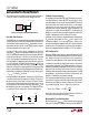
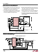
tor (see Figure 8), this noise will be minimized.
Figure 7. Minimum On-Time vs Inductor Ripple Current
INDUCTOR RIPPLE CURRENT (% OF I
MAX
)
0
200
MINIMUM ON-TIME (ns)
250
300
350
400
RECOMMENDED
REGION FOR MIN
ON-TIME AND
MAX EFFICIENCY
10 20 30 40
1435A F07
50 60 70
L
INDUCTOR
1435A F08
Figure 8. Allowable Inductor/R
SENSE
Layout Orientations
Efficiency Considerations
The efficiency of a switching regulator is equal to the out-
put power divided by the input power times 100%. It is often
useful to analyze individual losses to determine what is
limiting the efficiency and which change would produce the
most improvement. Efficiency can be expressed as:
Efficiency = 100% – (L1 + L2 + L3 + ...)
where L1, L2, etc. are the individual losses as a percentage
of input power.
Although all dissipative elements in the circuit produce
losses, four main sources usually account for most of the
losses in LTC1435A circuits. LTC1435A V
IN
current, INTV
CC
current, I
2
R losses, and topside MOSFET transition losses.
1. The V
IN
current is the DC supply current given in the
electrical characteristics which excludes MOSFET driver
and control currents. V
IN
current results in a small
(< 1%) loss which increases with V
IN
.
2. INTV
CC
current is the sum of the MOSFET driver and
control currents. The MOSFET driver current results from
switching the gate capacitance of the power MOSFETs.
Each time a MOSFET gate is switched from low to high
to low again, a packet of charge dQ moves from INTV
CC
to ground. The resulting dQ/dt is a current out of INTV
CC
that is typically much larger than the control circuit cur-
rent. In continuous mode, I
GATECHG
= f(Q
T
+ Q
B
), where
Q
T
and Q
B
are the gate charges of the topside and bot-
tom side MOSFETs.