
Datasheet

15
LTC1435A
APPLICATIONS INFORMATION
WUU
U
conduct during double battery operation, but must still
clamp the input voltage below breakdown of the converter.
Although the LTC1435A has a maximum input voltage of
36V, most applications will be limited to 30V by the
MOSFET BV
DSS
.
Design Example
As a design example, assume V
IN
= 12V(nominal), V
IN
=
22V(max), V
OUT
= 1.6V, I
MAX
= 3A and f = 250kHz, R
SENSE
and C
OSC
can immediately be calculated:
R
SENSE
= 100mV/3A = 0.033Ω
C
OSC
= 1.37(10
4
)/250 – 11 = 43pF
Referring to Figure 3, a 4.7µH inductor falls within the rec-
ommended range. To check the actual value of the ripple
current the following equation is used:
∆I
V
fL
V
V
L
OUT OUT
IN
=
()()
1–
The highest value of the ripple current occurs at the maxi-
mum input voltage:
∆I
V
kHz H
V
V
L
=
µ
()
=
16
250 4 7
1
16
22
13
.
.
–
.
.A
The lowest duty cycle also occurs at maximum input volt-
age. The on-time during this condition should be checked
to make sure it doesn’t violate the LTC1435A’s minimum
on-time and cause cycle skipping to occur. The required on-
time at V
IN(MAX)
is:
t
V
Vf
V
V kHz
ns
ON MIN
OUT
IN MAX
()
()
.
=
()()
=
()( )
=
16
22 250
291
The ∆I
L
was previously calculated to be 1.3A, which is 43%
of I
MAX
. From Figure 7, the LTC1435A minimum on-time
at 43% ripple is about 235ns. Therefore, the minimum on-
time is sufficient and no cycle skipping will occur.
The power dissipation on the topside MOSFET can be easily
estimated. Choosing a Siliconix Si4412DY results in:
R
DS(ON)
= 0.042Ω, C
RSS
= 100pF. At maximum input volt-
age with T(estimated) = 50°C:
P
V
V
CC
V A pF kHz mW
MAIN
=
()
+
()
°− °
()
[]
()
+
()()( )( )
=
16
22
3 1 0 005 50 25 0 042
2 5 22 3 100 250 88
2
185
.
..
.
.
Ω
The most stringent requirement for the synchronous
N-channel MOSFET occurs when V
OUT
= 0 (i.e. short cir-
cuit). In this case the worst-case dissipation rises to:
PI R
SYNC SC AVG DS ON
=
()
+
()
() ()
2
1
δ
With the 0.033Ω sense resistor I
SC(AVG)
= 4A will result,
increasing the Si4412DY dissipation to 950mW at a die tem-
perature of 105°C.
C
IN
is chosen for an RMS current rating of at least 1.5A at
temperature. C
OUT
is chosen with an ESR of 0.03Ω for low
output ripple. The output ripple in continuous mode will be
highest at the maximum input voltage. The output voltage
ripple due to ESR is approximately:
V
ORIPPLE
= R
ESR
(∆I
L
) = 0.03Ω(1.3A) = 39mV
P-P
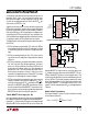
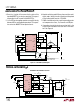
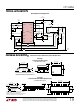
PC Board Layout Checklist
When laying out the printed circuit board, the following
checklist should be used to ensure proper operation of the
LTC1435A. These items are also illustrated graphically in
the layout diagram of Figure 10. Check the following in your
layout:
1. Are the signal and power grounds segregated? The
LTC1435A signal ground pin must return to the (–) plate
of C
OUT
. The power ground connects to the source of the
bottom N-channel MOSFET, anode of the Schottky di-
ode, and (–) plate of C
IN
, which should have as short lead
lengths as possible.
2. Does the V
OSENSE
pin connect directly to the feedback
resistors? The resistive divider R1, R2 must be con-
nected between the (+) plate of C
OUT
and signal ground.
The 100pF capacitor should be as close as possible to
the LTC1435A.
3. Are the SENSE
–
and SENSE
+
leads routed together with
minimum PC trace spacing? The filter capacitor between
SENSE
+
and SENSE
–
should be as close as possible to
the LTC1435A.