
Datasheet


4
LTC1448
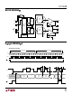
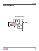
CLK (Pin 1): Serial Interface Clock. Internal Schmitt trig-
ger on this input allows direct optocoupler interface.
D
IN
(Pin 2): Serial Interface Data. Data on the D
IN
pin is
latched into the shift register on the rising edge of the serial
clock.
CS/LD (Pin 3): Serial Interface Enable and Load Control.
When CS/LD is low the CLK signal is enabled, so the data
can be clocked in. When CS/LD is pulled high, data is
loaded from the shift register into the DAC register,
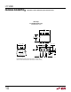
PIN FUNCTIONS
UUU
updating the DAC output and the CLK is disabled
internally.
REF (Pin 4): Reference Input for Both DACs. This pin can
be tied to V
CC
. The output will swing from 0V to REF. The
typical input resistance is 12.5k.
V
OUT A
, V
OUT B
(Pins 5, 8): Buffered DAC Outputs.
GND (Pin 6): Ground.
V
CC
(Pin 7): Positive Supply Input. 2.7V ≤ V
CC
≤ 5.5V.
Requires a bypass capacitor to ground.
TYPICAL PERFORMANCE CHARACTERISTICS
UW
LOAD CURRENT (mA)
0
V
CC
– V
OUT
(V)
51015
1448 G03
0.8
0.7
0.6
0.5
0.4
0.3
0.2
0.1
0
∆V
OUT
< 1LSB
CODE: ALL 1’s
V
OUT
= 4.095V
OUTPUT SINK CURRENT (mA)
0
OUTPUT PULL-DOWN VOLTAGE (mV)
51015
1448 G04
800
700
600
500
400
300
200
100
0
CODE: ALL 0’s
125°C
25°C
–55°C
Integral Nonlinearity (INL)
Minimum Supply Headroom for
Full Output Swing vs Load Current
Minimum Output Voltage vs
Output Sink Current
Supply Current vs
Logic Input Voltage
Differential Nonlinearity (DNL)
CODE
0
INL ERROR (LSB)
5
4
3
2
1
0
–1
–2
–3
–4
–5
1024
2048
2560
1448 G01
512 1536
3072
3584
4095
CODE
0
–0.5
DNL ERROR (LSB)
–0.4
–0.2
–0.1
0
0.5
0.2
1024 2048 2560
1448 TA02
–0.3
0.3
0.4
0.1
512 1536 3072 3584 4095
LOGIC INPUT VOLTAGE (V)
0
SUPPLY CURRENT (mA)
2.0
1.6
1.2
0.8
0.4
0
4
1448 G06
1
2
3
5