
Datasheet


3
LTC1451
LTC1452/LTC1453
V
CC
= 4.5V to 5.5V (LTC1451), 2.7V to 5.5V (LTC1452/LTC1453), internal or external reference (V
REF
≤ V
CC
/2), V
OUT
and REF
unloaded, T
A
= T
MIN
to T
MAX
, unless otherwise noted.
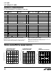
ELECTRICAL CHARACTERISTICS
SYMBOL PARAMETER CONDITIONS MIN TYP MAX UNITS
Reference (LTC1451/LTC1453)
Reference Output Voltage LTC1451
● 2.008 2.048 2.088 V
LTC1453 ● 1.195 1.220 1.245 V
Reference Output ±0.08 LSB/°C
Temperature Coefficient
Reference Line Regulation ● 0.7 ±2LSB/V
Reference Load Regulation 0 ≤ I
OUT
≤ 100µA, LTC1451 ● 0.2 ±1.5 LSB
LTC1453 ● 0.6 ±3 LSB
Reference Input Range V
REF
≤ V
CC
– 1.5V ● V
CC
/2 V
Reference Input Resistance ● 81430 kΩ
Reference Input Capacitance 15 pF
Short-Circuit Current REF Shorted to GND ● 80 mA
Power Supply
V
CC
Positive Supply Voltage For Specified Performance, LTC1451 ● 4.5 5.5 V
LTC1452
● 2.7 5.5 V
LTC1453 ● 2.7 5.5 V
I
CC
Supply Current 4.5V ≤ V
CC
≤ 5.5V (Note 4), LTC1451 ● 300 400 620 µA
2.7V ≤ V
CC
≤ 5.5V (Note 4), LTC1452 ● 120 225 350 µA
2.7V ≤ V
CC
≤ 5.5V (Note 4), LTC1453 ● 150 250 500 µA
Op Amp DC Performance
Short-Circuit Current Low V
OUT
Shorted to GND ● 100 mA
Short-Circuit Current High V
OUT
Shorted to V
CC
● 120 mA
Output Impedance to GND Input Code = 0 ● 40 120 Ω
AC Performance
Voltage Output Slew Rate (Note 2) ● 0.5 1.0 V/µs
Voltage Output Settling Time (Notes 2, 3) to ±0.5LSB 14 µs
Digital Feedthrough 0.3 nV• s
AC Feedthrough REF = 1kHz, 2V
P-P
, LTC1452 –95 dB
SINAD Signal-to-Noise + Distortion REF = 1kHz, 2V
P-P
, (Code: All 1s) LTC1452 85 dB