
Datasheet


6
LTC1480
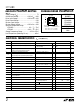
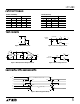
SWITCHI G TI E WAVEFOR S
UW W
Figure 6. Driver Enable and Disable Times
1.5V
2.3V
2.3V
t
ZH(SHDN)
,
t
ZH
t
ZL(SHDN)
,
t
ZL
1.5V
t
LZ
0.5V
0.5V
t
HZ
OUTPUT NORMALLY LOW
OUTPUT NORMALLY HIGH
3V
0V
DE
3.3V
V
OL
V
OH
0V
A, B
A, B
LTC1480 • F06
f = 1MHz, t
r
≤ 10ns, t
f
≤ 10ns
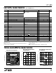
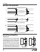
Figure 7. Receiver Propagation Delays
1.5V
t
PHL
RO
–V
OD2
A – B
0V 0V
1.5V
t
PLH
OUTPUT
INPUT
V
OD2
V
OL
V
OH
LTC1480 • F07
f = 1MHz, t
r
≤ 10ns, t
f
≤ 10ns
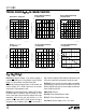
Figure 8. Receiver Enable and Disable Times
1.5V
t
ZL(SHDN)
, t
ZL
t
ZH(SHDN)
, t
ZH
1.5V
1.5V
1.5V
t
LZ
0.5V
0.5V
t
HZ
OUTPUT NORMALLY LOW
OUTPUT NORMALLY HIGH
3V
0V
RE
3.3V
V
OL
V
OH
0V
RO
RO
LTC1480 • F08
f = 1MHz, t
r
≤ 10ns, t
f
≤ 10ns
APPLICATIO S I FOR ATIO
UU W U
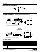
CMOS Output Driver
The LTC1480 transceiver provides full RS485 compatibil-
ity while operating from a single 3.3V supply. The RS485
specification requires that a transceiver withstand com-
mon-mode voltages of up to 12V or –7V at the RS485 line
connections. Additionally, the transceiver must be im-
mune to both ESD and latch-up, This rules out traditional
CMOS drivers, which include parasitic diodes from their
driver outputs to each supply rail (Figure 9). The LTC1480
uses a proprietary process enhancement which adds a
pair of Schottky diodes to the output stage (Figure 10),
preventing current from flowing when the common-mode
LOGIC
V
CC
P1
D1
OUTPUT
D2
N1
LTC1480 • F10
LOGIC
V
CC
SD3
P1
D1
OUTPUT
SD4
D2
N1
LTC1480 • F09
Figure 9. Conventional
CMOS Output Stage
Figure 10.
LTC1480 Output Stage