
Datasheet


7
LTC1480
APPLICATIO S I FOR ATIO
UU W U
receiver active and the driver outputs disabled, the LTC1480
will typically draw 300µA quiescent current. With the
driver outputs enabled but unterminated, quiescent cur-
rent will rise as one of the two outputs sources current into
the internal receiver input resistance. With the minimum
receiver input resistance of 12k and the maximum output
swing of 3.3V, the quiescent current will rise by a maxi-
mum of 275µA. Typical quiescent current rise with the
driver enabled is about 100µA.
The quiescent current rises significantly if the driver is
enabled when it is externally terminated. With 1/2 termina-
tion load (120Ω between the driver outputs) the quiescent
current will jump to at least 13mA as the drivers force a
minimum of 1.5V across the termination resistance. With
a fully terminated 60Ω line attached, the current will rise
to greater than 25mA with the driver enabled, completely
overshadowing the extra 100µA drawn by internal receiver
inputs.
Shutdown Mode
Both the receiver output (RO) and the driver outputs (A, B)
can be placed in three-state mode by bringing RE HIGH
and DE LOW respectively. In addition, the LTC1480 will
enter shutdown mode when RE is HIGH and DE is LOW.
In shutdown the LTC1480 typically draws only 1µA of
supply current. In order to guarantee that the part goes
into shutdown, RE must be high and DE must be LOW for
at least 600ns simultaneously. If this time duration is less
than 50ns the part will not enter shutdown mode.
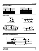
Propagation Delay
Many digital encoding schemes are dependent upon the
difference in the propagation delay times of the driver and
receiver. Figure 11 shows the test circuit for the LTC1480
propagation delay.
The receiver delay times are:
t
PLH
– t
PHL
= 13ns Typ, V
CC
= 3.3V
The driver’s skew times are:
t
SKEW
= 10ns Typ, V
CC
= 3.3V
20ns Max, V
CC
= 3.3V, T
A
= –40°C to 85°C
voltage exceeds the supply rails. Latch-up at the output
drivers is virtually eliminated and the driver is prevented
from loading the line under RS485 specified fault condi-
tions. A proprietary output protection structure protects
the transceiver line terminals against ESD strikes of up to
±10kV.
When two or more drivers are connected to the same
transmission line, a potential condition exists whereby
more than two drivers are simultaneously active. If one or
more drivers is sourcing current while another driver is
sinking current, excessive power dissipation may occur
within either the sourcing or sinking element. This condi-
tion is defined as driver contention, since multiple drivers
are competing for one transmission line. The LTC1480
provides a current limiting scheme to prevent driver
contention failure. When driver contention occurs, the
current drawn is limited to about 70mA preventing exces-
sive power dissipation within the drivers.
The LTC1480 has a thermal shutdown feature which
protects the part from excessive power dissipation. Under
extreme fault conditions, up to 250mA can flow through
the part causing rapid internal temperature rise. The
thermal shutdown circuit will disable the driver outputs
when the internal temperature reaches 150°C and turns
them back on when the temperature cools to 130°C. This
cycle will repeat as necessary until the fault condition is
removed.
Receiver Inputs
The LTC1480 features an input common-mode range
covering the entire RS485 specified range of –7V to 12V.
Differential signals of greater than ±200mV within the
specified input common-mode range will be converted to
a TTL compatible signal at the receiver output. A small
amount of input hysteresis is included to minimize the
effects of noise on the line signals. If the receiver inputs are
floating (unterminated) an internal pull-up of 10µA at the
A input will force the receiver output to a known high state.
Low Power Operation
The LTC1480 draws very little supply current whenever
the driver outputs are disabled. In shutdown mode the
quiescent current is typically less than 1µA. With the
Information furnished by Linear Technology Corporation is believed to be accurate and reliable.
However, no responsibility is assumed for its use. Linear Technology Corporation makes no represen-
tation that the interconnection of circuits as described herein will not infringe on existing patent rights.